 ALLPCB


Introduction
High-frequency applications continue to push printed circuit boards toward smaller footprints while demanding reliable signal performance. Engineers working with RF circuits and high-speed digital interfaces often face the challenge of fitting complex routing into limited board real estate without compromising transmission quality. Minimum size RF PCB designs require careful attention to every layout decision because even small changes in trace geometry or layer arrangement can alter electrical behavior. Signal integrity in small PCBs becomes a primary constraint when board dimensions shrink and operating frequencies rise into the gigahertz range. Successful projects balance physical size reduction with electrical requirements through systematic planning of stackup, materials, and routing rules.
Why Minimum Size Matters in High-Frequency PCB Design
Reducing PCB dimensions lowers material costs and enables compact end products such as portable communication devices and embedded sensors. At the same time, smaller boards increase the density of traces and components, which heightens the risk of electromagnetic coupling between adjacent signals. Impedance control small PCB layouts must maintain consistent characteristic impedance despite shorter trace lengths and tighter spacing. RF PCB design constraints become more stringent because wavelength shortening at higher frequencies makes every discontinuity more significant relative to signal period. Designers therefore treat board size as an optimization variable that directly influences both manufacturing yield and functional reliability.
Technical Principles of Signal Integrity in Compact Layouts
In high-frequency regimes, traces behave as transmission lines rather than simple conductors, so reflections and standing waves appear when impedance mismatches occur. Skin effect concentrates current near conductor surfaces, raising effective resistance and contributing to attenuation that grows with frequency. Crosstalk arises from mutual inductance and capacitance between neighboring traces, and this coupling strengthens when spacing decreases to accommodate smaller board outlines. Dielectric losses in the substrate also increase with frequency, requiring selection of materials whose loss tangent remains low across the operating band. Via transitions introduce inductance and capacitance that can create resonances, particularly when the board thickness is comparable to a fraction of the signal wavelength.
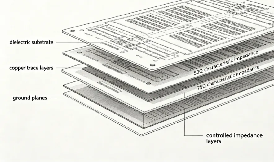
Parasitic effects from component pads and solder joints further complicate the picture because their physical size does not scale proportionally with overall board shrinkage. Ground return paths must remain continuous and low-inductance to prevent voltage drops that modulate signal levels. Thermal considerations also enter the analysis because power dissipation in small areas raises local temperatures that can alter material properties and accelerate aging.
Practical Design Approaches for Maintaining Performance
Engineers begin by defining target impedance values early in the project and then selecting dielectric thickness and trace width combinations that achieve those values within manufacturing tolerances. Differential pair routing maintains tight coupling and equal lengths to preserve signal balance while fitting within narrow board margins. Ground planes placed adjacent to signal layers provide the necessary return paths and help contain electromagnetic fields. Stitching vias along board edges and around sensitive circuits reduce cavity resonances that otherwise appear in compact enclosures.
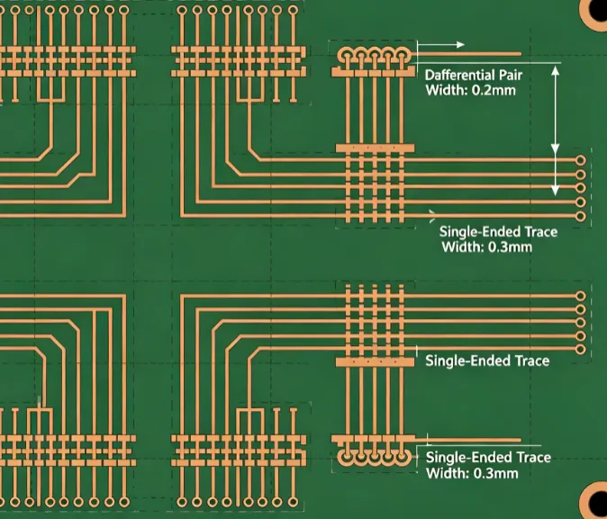
Component placement follows a logical sequence that groups high-speed devices together and keeps analog sections separated from digital noise sources. Decoupling capacitors are positioned as close as possible to power pins, with multiple vias connecting each capacitor to the reference plane to minimize loop inductance. Trace corners use smooth curves or 45-degree mitered bends rather than sharp right angles to limit radiation and reflection. Test points and probe pads are added only where essential and are sized to avoid creating additional discontinuities.
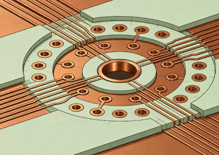
Design rule checks incorporate both electrical and manufacturing limits, verifying minimum annular ring sizes, copper-to-copper clearances, and drill aspect ratios that remain feasible for the chosen board thickness. Iterative simulation of the full layout, including extracted parasitics, confirms that signal integrity metrics such as eye opening and return loss stay within acceptable bounds before fabrication.
Conclusion
Compact high-frequency PCB designs succeed when size reduction is pursued alongside rigorous control of impedance, crosstalk, and parasitic elements. Logical sequencing of stackup decisions, material choices, and routing practices allows engineers to meet both mechanical and electrical targets. Attention to via design, ground integrity, and component placement further reduces the likelihood of performance degradation. These principles, applied consistently, support reliable operation in space-constrained RF and high-speed applications.
FAQs
Q1: How does board size affect impedance control in high-frequency designs?
A1: Smaller board dimensions force tighter trace spacing and shorter lengths, which can alter the effective dielectric environment and make it harder to maintain target impedance values. Consistent stackup planning and trace geometry calculations help preserve the required characteristic impedance despite the reduced footprint.
Q2: What are the main RF PCB design constraints when minimizing board size?
A2: Key constraints include maintaining adequate trace-to-trace spacing to limit crosstalk, ensuring continuous low-inductance return paths, and managing via inductance that becomes proportionally larger in thin, compact boards. Frequency-dependent losses and thermal concentration also require explicit consideration during layout.
Q3: Why is signal integrity harder to achieve in small PCBs operating at high frequencies?
A3: Reduced physical separation increases electromagnetic coupling between signals, while shorter wavelengths make every geometric discontinuity more electrically significant. Parasitic inductance and capacitance from vias and pads can create resonances that fall within the operating band when board dimensions shrink.
Q4: What layout practices help preserve signal quality in minimum size RF PCBs?
A4: Controlled impedance routing, adjacent ground planes, dense via stitching, and careful component grouping all contribute to stable transmission characteristics. Simulation of the complete interconnect before fabrication verifies that reflections and crosstalk remain within acceptable limits.
References
IPC-2221B — Generic Standard on Printed Board Design. IPC, 2012
IPC-6012E — Qualification and Performance Specification for Rigid Printed Boards. IPC, 2017
IPC-A-600K — Acceptability of Printed Boards. IPC, 2020





