 ALLPCB


Introduction
Industrial automation controllers rely on printed circuit boards (PCBs) to manage complex signals in harsh electromagnetic environments. Electromagnetic interference (EMI) poses a significant threat to these systems, potentially causing signal corruption, erratic behavior, or complete failure. Effective mitigation strategies are essential to ensure reliable operation amid motors, power supplies, and sensors that generate noise. PCB EMI shielding techniques form the cornerstone of defense, combining layout optimization, grounding, and filtering. This article explores structured approaches to reduce EMI, emphasizing grounding strategies for EMI reduction and signal filtering for sustained performance. Engineers designing for automation must prioritize these methods to meet operational demands.
Understanding EMI and Its Impact on Industrial PCBs
Electromagnetic interference refers to unwanted noise that disrupts electronic circuits through conduction or radiation. In industrial settings, controllers process high-speed digital signals alongside analog inputs from sensors, making them vulnerable to EMI from nearby equipment. Conducted EMI travels via power lines or cables, while radiated EMI propagates through air as electromagnetic waves. Failure to address these can lead to data errors, reduced uptime, and safety risks in automation systems. Noise reduction in industrial PCBs demands a holistic design approach from stackup to component placement. Compliance with standards like IPC-2221C ensures designs withstand real-world stresses.
Industrial automation PCBs operate in environments with variable frequencies and intensities of interference. Motors induce high-frequency noise, inverters generate harmonics, and switching power supplies emit broadband emissions. These factors amplify susceptibility, where even minor coupling alters control logic. Quantifying EMI requires understanding field strengths and coupling paths, guiding mitigation priorities. Engineers must balance performance, cost, and manufacturability while targeting root causes.
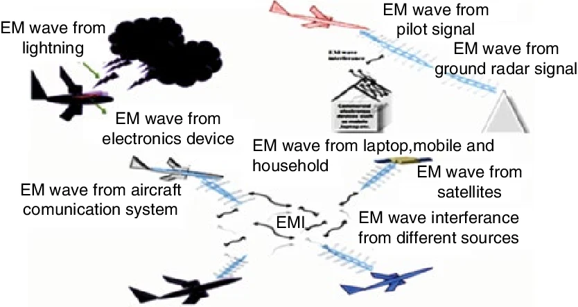
Mechanisms of EMI Generation and Propagation
EMI originates from rapid voltage or current changes creating time-varying fields. Clock signals in microcontrollers produce harmonics that radiate if loop areas are large. Poor return paths force currents to spread, increasing emissions. Capacitive and inductive coupling between traces exacerbates crosstalk within the PCB. External fields induce voltages on loops, compromising signal integrity. Analyzing these mechanisms reveals opportunities for intervention at the design stage.
Propagation modes differ: near-field effects dominate close to sources, transitioning to far-field radiation. Impedance mismatches reflect signals, amplifying noise. Ground bounce from simultaneous switching further pollutes references. Thermal and mechanical stresses can degrade shielding over time. Structured simulation aids prediction, but empirical validation confirms effectiveness.
PCB EMI Shielding Techniques
PCB EMI shielding techniques enclose sensitive areas to block fields. Dedicated ground planes act as shields by providing low-impedance return paths and image currents that cancel emissions. Multi-layer boards dedicate inner layers to ground, isolating signal layers. Guard traces or rings around critical nets divert stray fields. These methods reduce radiated emissions by minimizing aperture sizes in the layout.
Shielding cans or enclosures cover noisy sections, grounded at multiple points for effectiveness. Conductive gaskets ensure continuity across seams. For high-frequency threats, metalized paints or films on enclosures enhance attenuation. Layer stackup symmetry prevents warpage while optimizing shielding. Placement of shields requires thermal vias to manage heat dissipation.
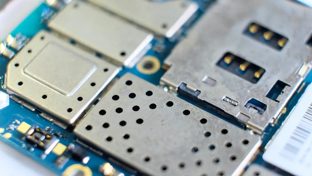
Via stitching connects ground planes, creating a Faraday cage effect. Stitching density depends on wavelength, typically every lambda/20. This technique suppresses slot antennas formed by plane splits. Combining planes with moats channels currents predictably.
Grounding Strategies for EMI Reduction
Grounding strategies for EMI reduction start with a solid plane rather than spokes or stars, which create inductance. A contiguous plane equalizes potentials, minimizing voltage drops under load. Split planes for analog and digital domains prevent noise crossover, connected via narrow bridges near ICs. Single-point grounding suits low-frequency, while multi-point fits high-speed designs.
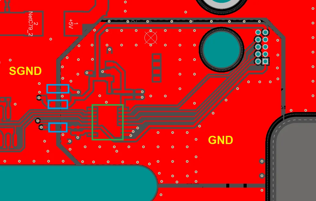
Return current paths must align with forward traces to shrink loops. Probing ground noise reveals hotspots for refinement. Dynamic grounding adapts to operating modes via relays, though static designs prevail in controllers.
Signal Filtering and Noise Reduction in Industrial PCBs
Signal filtering employs capacitors, inductors, and ferrites to attenuate unwanted frequencies. Pi-filters near connectors block conducted EMI effectively. Ferrite beads on cables absorb common-mode noise without affecting differential signals. Bypass capacitors across supplies decouple ICs, with values selected for resonance at clock harmonics.
Active filtering integrates op-amps for precise cutoffs in analog paths. Spread-spectrum clocking modulates edges to lower peak emissions. Differential signaling rejects common-mode noise inherently. These complement passive methods for comprehensive noise reduction in industrial PCBs.
Achieving EMC Compliance in PCB Design
EMC compliance in PCB design integrates shielding, grounding, and filtering from schematic to fabrication. Pre-compliance testing with spectrum analyzers identifies issues early. Board size and edge terminations affect radiation patterns. Compliance margins account for production variations.
Adhering to IPC-2221C for spacing and plane design supports IEC 61000-6-2 immunity levels. Documentation traces decisions to requirements. Iterative prototyping refines layouts.
Best Practices for Implementation
Layer count influences shielding: four-layer minimum for controllers separates signals from planes. Trace routing avoids 90-degree bends, using 45-degree for smoother fields. Clock lines over ground planes with minimal vias. Component orientation aligns noisy parts away from edges.
Thermal management integrates with EMI via heatsinks that double as shields. Documentation specifies shielding materials compatible with assembly.
Conclusion
Mitigating EMI in industrial automation controller PCBs demands integrated PCB EMI shielding techniques, grounding strategies for EMI reduction, and signal filtering. These ensure reliable operation amid harsh noise. EMC compliance in PCB design follows from principled layouts per industry standards. Noise reduction in industrial PCBs enhances longevity and performance. Engineers achieve success through systematic application, balancing trade-offs effectively.
FAQs
Q1: What are the most effective PCB EMI shielding techniques for industrial controllers?
A1: PCB EMI shielding techniques include ground planes, shielding cans, and guard rings to block radiated fields. Multi-layer stackups isolate signals, while via stitching creates cage-like barriers. These reduce emissions and susceptibility in noisy environments. Implementation follows logical partitioning for optimal results.
Q2: How do grounding strategies for EMI reduction improve PCB performance?
A2: Grounding strategies for EMI reduction use solid planes to minimize inductance and equalize potentials. Split domains prevent noise migration between analog and digital sections. Multi-point connections suit high frequencies, aligning with IEC 61000-6-2. Proper execution lowers emissions significantly.
Q3: Why is EMC compliance in PCB design critical for automation systems?
A3: EMC compliance in PCB design prevents interference in industrial settings with motors and inverters. It ensures signal integrity and regulatory adherence via shielding and filtering. Standards like IPC-2221C guide layouts for immunity. Non-compliance risks failures and downtime.
Q4: What role does signal filtering play in noise reduction in industrial PCBs?
A4: Signal filtering uses pi-networks and ferrites to suppress conducted EMI on power lines. Placement near ICs or connectors maximizes attenuation. This complements shielding for broadband protection. Engineers select components for target frequencies effectively.
References
IPC-2221C — Generic Standard on Printed Board Design. IPC, 2023
IEC 61000-6-2 — Electromagnetic compatibility (EMC) - Part 6-2: Generic standards - Immunity for industrial environments. IEC, 2016





