 ALLPCB


Reducing Warping During Manufacturing
PCB warping during manufacturing remains a critical challenge for electric engineers designing high-reliability boards. Warpage, which includes bow and twist, arises from internal stresses that develop as the board cools after lamination and reflow processes. These distortions can misalign pads, complicate component placement, and reduce long-term mechanical integrity. Engineers address the issue primarily through careful PCB stackup design that balances mechanical and thermal properties across all layers. Effective control begins at the design stage and extends through material selection and process parameters.
What Is PCB Warping and Why It Matters
PCB warping describes the out-of-plane deformation that occurs when a printed circuit board deviates from flatness. Bow typically appears as a cylindrical curvature along one axis, while twist produces a saddle-like or helical shape. Industry standards define acceptable limits based on board thickness and application requirements. For multilayer constructions, even minor deviations become problematic because they compound with increasing layer count PCB. Electric engineers must account for these effects early because excessive warpage interferes with automated assembly equipment and can create stress concentrations at solder joints. The problem grows more pronounced in boards with higher layer counts or mixed-signal designs where signal integrity and mechanical stability must coexist.
Technical Principles and Mechanisms
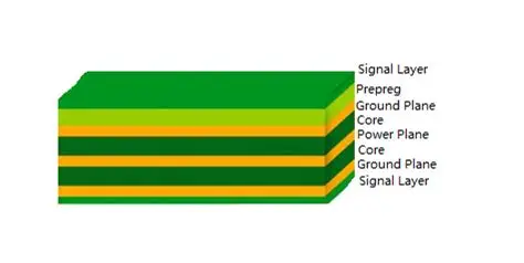
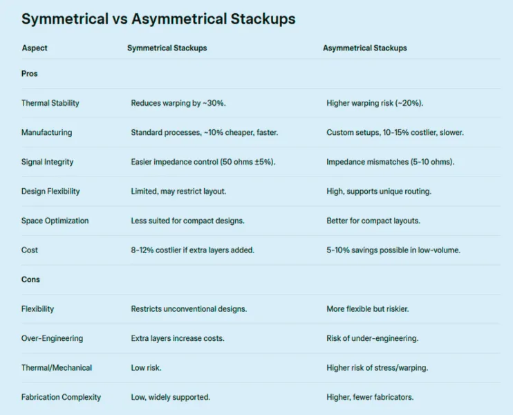
Warping originates from mismatched coefficients of thermal expansion (CTE) between copper, dielectric materials, and reinforcements within the stackup. During cooling after lamination, the outer layers contract at different rates than inner layers, generating residual stresses. An asymmetrical PCB stackup design exacerbates this imbalance because the neutral axis shifts away from the geometric center. Copper distribution also plays a decisive role; heavy copper on one side relative to the other creates localized shrinkage differences. PCB reference plane placement influences both electrical performance and mechanical symmetry. When reference planes sit unevenly or lack balanced copper weight, they contribute to twisting moments. Moisture absorption prior to processing adds another variable, as trapped vapor expands during heating and further distorts the laminate. Layer count PCB directly affects complexity because each additional core or prepreg introduces new interfaces where stress can accumulate.
Practical Solutions and Best Practices
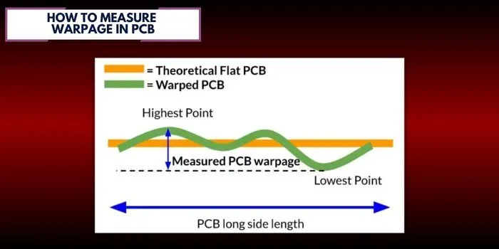
Electric engineers reduce PCB warping during manufacturing by enforcing symmetrical stackup design from the outset. This approach places identical dielectric thicknesses, copper weights, and material types in mirror-image positions above and below the center of the board. A well-executed symmetrical stackup keeps the neutral axis centered, minimizing bending moments during thermal excursions. Designers also balance copper area on PCB reference planes so that each plane carries equivalent copper density on opposite sides of the stackup. When signal layers require different copper weights, compensation occurs through careful distribution of dummy copper or adjusted reference plane fills. Layer count PCB decisions should favor even numbers of layers when possible, allowing natural pairing of cores and prepregs. Process controls further support these design measures by maintaining consistent lamination pressure, temperature profiles, and cooling rates. Engineers verify compliance with flatness requirements through standardized measurement methods after fabrication.
Additional mitigation comes from specifying materials with closely matched CTE values throughout the stackup. Controlled expansion laminates help keep overall board movement within acceptable bounds even when layer count PCB increases. During layout, engineers route high-copper-density areas such as power planes to avoid clustering on one side. Post-lamination baking removes absorbed moisture before subsequent thermal steps, reducing the risk of vapor-induced distortion. Final inspection includes bow-and-twist measurements taken at multiple points across the panel to confirm that the finished boards meet the flatness criteria established for the intended assembly process.
Conclusion
Reducing PCB warping during manufacturing requires integrated attention to PCB stackup design, copper balance on PCB reference planes, and overall layer count PCB considerations. Symmetrical constructions provide the most reliable foundation for maintaining flatness across thermal cycles. When these principles guide the design process, boards exhibit improved dimensional stability that supports both assembly yield and long-term reliability. Electric engineers who apply these structured approaches consistently achieve better outcomes without relying on post-fabrication corrections.
FAQs
Q1: How does symmetrical stackup design help control PCB warping during manufacturing?
A1: A symmetrical stackup places identical materials and copper weights in mirror positions around the board centerline. This configuration keeps the neutral axis centered and reduces differential contraction forces that cause bow and twist. Electric engineers routinely adopt this approach for multilayer boards to maintain flatness through lamination and reflow.
Q2: What role does the PCB reference plane play in minimizing warpage?
A2: PCB reference planes contribute to both electrical return paths and mechanical balance. When copper distribution on these planes remains balanced on opposite sides of the stackup, the board experiences lower internal stresses during cooling. Proper placement and fill patterns therefore support both signal integrity and reduced deformation.
Q3: Why does increasing layer count PCB raise the risk of warping?
A3: Higher layer count PCB introduces more interfaces between dissimilar materials, each with its own CTE. Without symmetrical pairing of cores and prepregs, these interfaces generate cumulative stresses that manifest as greater bow or twist. Careful stackup planning becomes essential as layer count grows.
Q4: Can material selection alone prevent PCB warping during manufacturing?
A4: Material choice influences overall CTE behavior but cannot compensate for an asymmetrical stackup or unbalanced copper distribution. Engineers combine appropriate laminate properties with symmetrical PCB stackup design and balanced reference planes to achieve the best control over warpage.
References
JEDEC J-STD-020E — Moisture/Reflow Sensitivity Classification. JEDEC, 2014


