 ALLPCB


Introduction
Power planes form the backbone of power distribution in multilayer PCBs, enabling reliable operation in high-performance electronic designs. These dedicated copper layers handle more current than traditional traces, distribute power efficiently across the board, and support complex circuitry. By keeping the voltage stable and minimizing drops under load, power planes ensure components receive consistent supply. They also reduce noise and heat, which are critical for maintaining signal integrity and thermal reliability. In this article, we examine the key functions of power planes from an engineering perspective, focusing on their role in enhancing performance in multilayer PCBs. Understanding these functions allows electric engineers to optimize designs for demanding applications.
What Are Power Planes and Why Do They Matter?
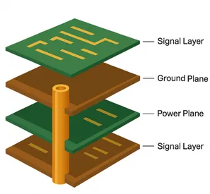
Power planes are extensive copper areas, typically full pours on inner layers of multilayer PCBs, dedicated to power or ground distribution. Unlike narrow signal traces, they span the entire board or large sections, providing a low-impedance path for current flow. In multilayer PCBs, power planes occupy specific layers between signal routings, allowing dense integration of components while separating power from sensitive signals. This structure matters because modern electronics demand high current delivery without excessive voltage fluctuations or electromagnetic interference.
The relevance stems from the limitations of trace-based power delivery in high-performance systems. Traces suffer from higher resistance and inductance, leading to voltage drops and instability as current increases. Power planes address this by offering a broad conductive surface that handles more current effectively. They also contribute to overall board performance by reducing noise and heat buildup, which can degrade signals and cause failures. For electric engineers designing multilayer PCBs, incorporating power planes is essential for meeting reliability targets in applications like power supplies and computing hardware.
Key Functions of Power Planes
Handling More Current
Power planes excel at handling more current compared to traces due to their large cross-sectional area, which significantly lowers DC resistance. The resistance of a conductor follows the formula R = ρL / A, where ρ is resistivity, L is length, and A is the cross-sectional area; planes maximize A across the board width. This capability supports high-power components without overheating narrow paths. In multilayer PCBs, multiple power planes can share current loads via vias, distributing thermal stress evenly.
According to IPC-2152, current-carrying capacity depends on copper thickness, temperature rise, and plane geometry, guiding engineers in sizing planes appropriately. Voids or splits in planes must be minimized to avoid current crowding, which could exceed safe limits. This function directly boosts performance by enabling higher power densities in compact designs. Electric engineers benefit from simulating current distribution to verify plane adequacy during the design phase.
Keeping the Voltage Stable
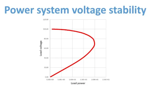
Power planes keep the voltage stable by minimizing inductance and resistance in the power delivery network. Inductance in traces causes voltage spikes or droops during transient loads, but planes reduce loop inductance through their planar geometry and proximity to ground planes. The voltage drop ΔV = IR + L di/dt becomes negligible with low R and L values inherent to planes. Decoupling capacitors placed near loads further enhance stability by supplying local charge.
In multilayer PCBs, adjacent power and ground planes form a low-impedance capacitor, suppressing ripple and maintaining steady supply. This stability is crucial for analog and digital circuits sensitive to variations. Engineers must ensure uniform plane thickness per IPC-2221C guidelines to avoid localized drops. Overall, this function prevents performance degradation and ensures compliance with system timing requirements.
Reducing Noise
Power planes reduce noise by providing a low-impedance return path for signals, particularly ground planes that shield sensitive traces. Electromagnetic interference arises from unbalanced current loops, but planes offer a broad reference plane, minimizing loop areas and radiated emissions. This containment of return currents prevents crosstalk between layers in multilayer PCBs. Solid ground planes also absorb switching noise from power circuits.
The effectiveness increases with plane continuity and via stitching, which ties planes to components. Per design standards, fragmented planes introduce inductance that amplifies noise. Electric engineers observe reduced EMI in prototypes with well-implemented planes during compliance testing. This noise reduction enhances signal-to-noise ratios, vital for high-speed interfaces.
Dissipating Heat
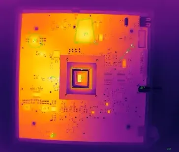
Power planes reduce heat by spreading thermal energy across a large copper area, acting as heat spreaders and sinks. High currents generate I2R losses, concentrated in traces but dissipated broadly in planes. The thermal conductivity of copper, around 400 W/m·K, allows efficient conduction to board edges or heatsinks. In multilayer PCBs, stacked planes create thermal vias paths for vertical heat flow.
Thinner dielectrics between planes improve heat transfer to outer layers. Engineers calculate temperature rise using IPC-2221C thermal relief patterns for vias connecting to planes. This function prevents hotspots that warp boards or degrade components. By managing heat alongside electrical functions, power planes sustain long-term performance.
Technical Principles of Power Planes
The core principle behind power planes lies in their geometry optimizing electrical and thermal parameters. At DC, resistance scales inversely with width, making planes far superior for handling more current. At higher frequencies, skin effect confines current to the surface, but plane thickness compensates effectively. Inductance per unit length drops with wider conductors, keeping the voltage stable even under fast transients.
Capacitance between power and ground planes, C = εA/d, provides distributed filtering, reducing noise. Engineers model these using field solvers to predict behavior in multilayer PCBs. Standards like IPC-6012F specify minimum copper weights and plating for performance qualification. These principles ensure planes deliver on performance promises without fabrication compromises.
Best Practices for Power Plane Implementation
Start with solid pours avoiding unnecessary splits that increase impedance. Use via stitching every 1/10 wavelength or 50-100 mils for current sharing and heat transfer. Place decoupling capacitors directly on planes via short vias to bypass noise. In multilayer PCBs, dedicate inner layers to power and ground for shielding.
Simulate current density to identify hotspots per IPC-2152 guidelines. Maintain clearance around splits for voltage isolation. Fabricate with heavier copper, like 2 oz/ft2, for high-current needs. These practices maximize benefits while mitigating risks like warping from uneven plating.
Troubleshooting Power Plane Issues
Common issues include voids from plating defects, causing current hotspots and voltage instability. Inspect per IPC-6012F for uniformity. Splits near high-speed signals introduce noise; redesign with moats only where necessary. Overheating signals poor stitching; add more vias.
Measure plane resistance post-fabrication to verify integrity. Simulate before build to predict problems. Addressing these ensures reliable performance in multilayer PCBs.
Conclusion
Power planes are indispensable for high-performance multilayer PCBs, handling more current, keeping the voltage stable, and reducing noise and heat effectively. Their structured implementation follows proven engineering principles and standards. Electric engineers gain substantial benefits in reliability and efficiency by prioritizing these functions. Mastering power planes elevates design quality, supporting advanced electronics demands.
FAQs
Q1: How do power planes handle more current in multilayer PCBs?
A1: Power planes handle more current through their expansive copper area, which reduces resistance compared to traces. This large cross-section supports high amperage without excessive voltage drop or heating. Standards like IPC-2152 guide capacity calculations based on copper weight and temperature rise. In multilayer PCBs, via arrays distribute loads evenly, enhancing overall performance.
Q2: In what ways do power planes keep the voltage stable?
A2: Power planes keep the voltage stable by offering low inductance paths and forming capacitance with ground planes. This minimizes droops during load changes and filters ripple. Proximity in multilayer stacks further lowers impedance. Decoupling enhances local stability, ensuring consistent supply for sensitive components.
Q3: How do power planes reduce noise and heat?
A3: Power planes reduce noise via solid return paths that contain EMI and shield signals. Ground planes absorb switching transients effectively. For heat, copper spreads I2R losses, preventing hotspots. In multilayer PCBs, thermal vias aid dissipation, improving reliability and performance.
Q4: Why are power planes critical for performance in multilayer PCBs?
A4: Power planes boost performance by enabling high current handling, voltage stability, and noise/heat reduction in dense multilayer PCBs. They free signal layers for routing while maintaining integrity. Adhering to IPC-2221C ensures optimal design. This integration supports faster, more reliable systems.
References
IPC-2221C — Generic Standard on Printed Board Design. IPC, 2023
IPC-2152 — Standard for Determining Current Carrying Capacity in Printed Board Design. IPC
IPC-6012F — Qualification and Performance Specification for Rigid Printed Boards. IPC, 2023





