ALLPCB


Introduction
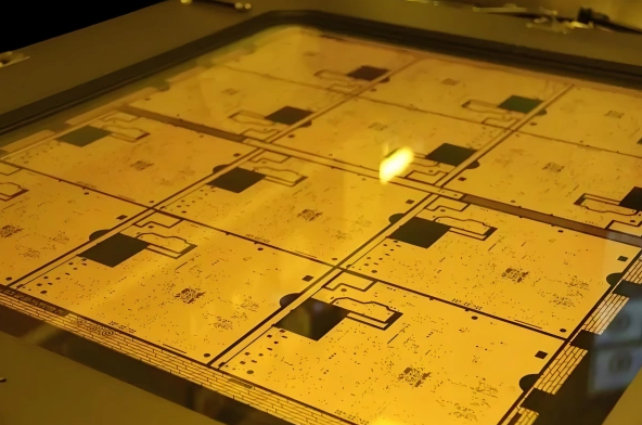
Power integrity in FR-4 PCBs forms the foundation for reliable operation in electronic systems where stable voltage delivery directly impacts performance. FR-4, a glass-reinforced epoxy laminate, remains the most common substrate due to its balance of mechanical strength, cost-effectiveness, and electrical properties suitable for a wide range of applications. However, as circuit speeds increase and component densities rise, challenges like voltage fluctuations, noise coupling, and impedance mismatches become prominent in FR-4 PCB power distribution networks. Engineers must address these issues through careful design of power and ground planes, along with strategic component placement, to prevent signal degradation and system failures. This article explores the principles and best practices for achieving robust FR-4 PCB power integrity, tailored for electrical engineers seeking structured guidance.
Understanding FR-4 PCB Power Integrity
FR-4 PCB power integrity refers to the ability of the power distribution network to deliver clean, stable DC power to all components without excessive voltage drop or noise injection. It encompasses the entire path from the voltage regulator to the load, including planes, traces, vias, and decoupling elements. Poor power integrity manifests as ripple on supply lines, which can couple into signals and cause timing errors or logic upsets. In FR-4 materials, the dielectric constant around 4.0 to 4.7 and moderate loss tangent influence plane capacitance and impedance, making targeted design essential. Why does it matter? In high-density boards, even minor deviations in voltage can lead to electromagnetic interference or thermal hotspots, compromising overall system reliability.
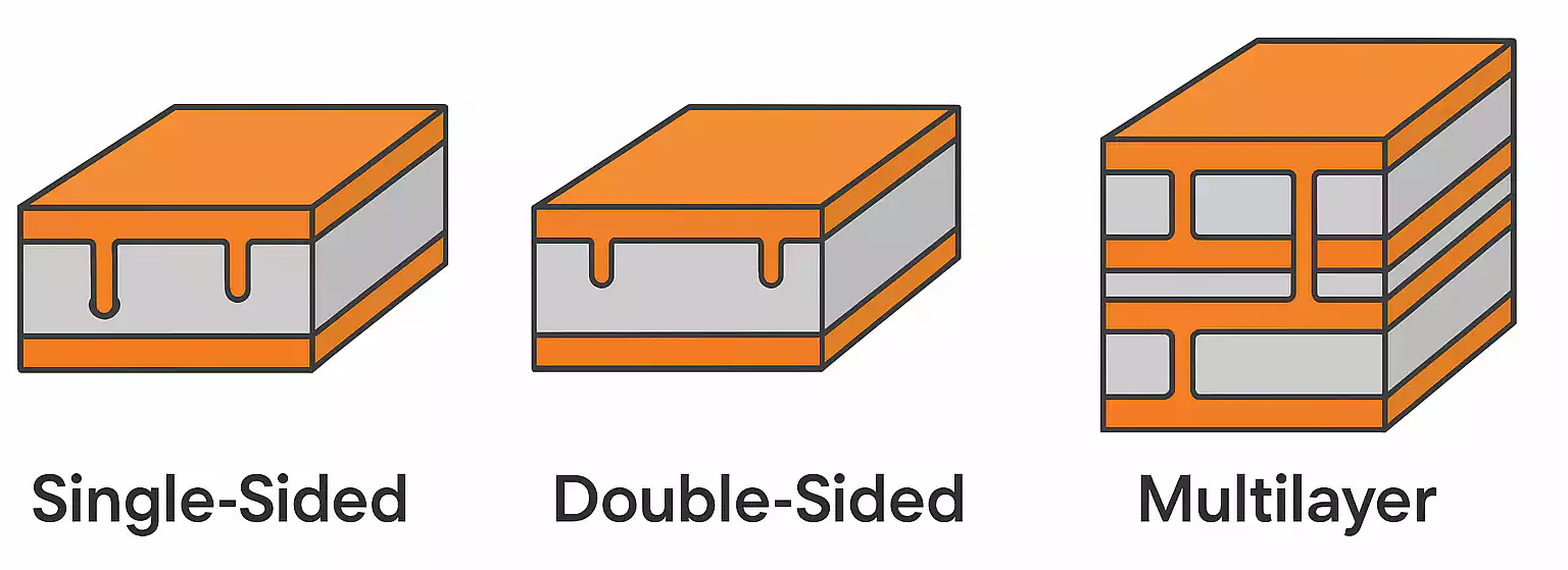
Core Elements of the FR-4 PCB Power Distribution Network
The power distribution network in FR-4 PCBs integrates power planes, ground planes, and decoupling capacitors to form a low-impedance path for both DC and transient currents. Power planes distribute voltage across large areas with minimal resistance, while ground planes provide return paths that minimize loop inductance. Decoupling capacitors bridge high-frequency transients by storing and releasing charge locally. Voltage drop, or IR drop, occurs due to resistive losses in conductors, exacerbated in thinner FR-4 cores under high current loads. Noise reduction relies on plane pairing and capacitive shunting to suppress simultaneous switching noise. Together, these elements ensure the PDN impedance stays below target levels across frequencies from DC to GHz.
Related Reading: Power Integrity and PCB Stackups: Optimizing Power Distribution Networks
FR-4 PCB Power Plane Design Principles
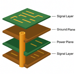
Effective FR-4 PCB power plane design starts with dedicating full copper layers to power distribution, typically 1 or 2 oz/ft2 thickness for standard applications. Continuous planes reduce DC resistance and provide distributed capacitance with adjacent dielectrics in FR-4. Avoid splits under high-current components to prevent current crowding and hotspots; instead, use stitching vias around splits for redundancy. Per IPC-2221 guidelines, calculate plane widths and thicknesses based on current density to limit temperature rise. Layer stackup positioning matters: place power planes adjacent to ground for tight coupling and lower inductance. This approach minimizes FR-4 PCB voltage drop and supports higher frequencies where skin effect dominates.

Optimizing FR-4 PCB Ground Plane Design
A solid ground plane in FR-4 PCBs serves as the reference for all signals and a low-impedance sink for return currents, critical for FR-4 PCB noise reduction. Design it as a full pour on inner layers, avoiding traces that fragment the plane and increase inductance. Stitch ground vias densely around board edges and component perimeters to equalize potentials and suppress slot resonances. In multilayer FR-4 stackups, pair each signal layer with a nearby ground plane to contain return paths and reduce crosstalk. Ground plane splits should mirror power splits exactly, connected via multiple vias to maintain continuity. This configuration enhances the overall FR-4 PCB power distribution network by lowering PDN impedance at high frequencies.
Related Reading: Mastering PDN Impedance: A Comprehensive Guide for Power Integrity Design
Mitigating Voltage Drop in FR-4 PCBs
Voltage drop in FR-4 PCBs arises from ohmic losses in power delivery paths, particularly under dynamic loads where current spikes demand low resistance. Thicker copper planes and wider traces compensate for FR-4's moderate thermal conductivity, keeping drops below 5% of supply voltage. Model DC IR drop using sheet resistance formulas, factoring in via counts and plane areas. For high-current rails, segment planes with decoupling to balance loads. Transient voltage drops require low-inductance paths, achieved by minimizing via lengths in FR-4 vias. Regular simulation verifies compliance before fabrication.
Strategies for FR-4 PCB Noise Reduction
FR-4 PCB noise reduction hinges on suppressing power supply ripple and switching transients through layered defenses. Decoupling capacitors, placed within millimeters of IC power pins, provide local charge reservoirs for high di/dt events. Use a mix of values: 0.1 μF ceramics for mid-frequencies and bulk electrolytics for low-end filtering. Plane capacitance in FR-4 stackups inherently bypasses some noise, augmented by embedded caps if needed. Ferrite beads on supply lines further isolate low-frequency noise. These techniques collectively target PDN target impedance curves for quiet power delivery.
Best Practices for FR-4 PCB Power Integrity
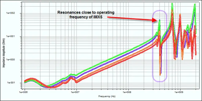
Adopt a 4-layer or higher stackup for FR-4 PCBs: signal over power, ground over signal, to optimize coupling. Follow IPC-2221 for conductor sizing and IPC-6012 for performance qualification in power planes. Place decoupling capacitors on the component side, vias immediately adjacent, forming pi-filters with plane inductance. Simulate PDN impedance early, targeting <10 mΩ at frequencies up to 1 GHz. Control FR-4 warpage during lamination to preserve plane flatness. Validate with scope measurements post-assembly for voltage ripple and eye diagrams.
- Adjacent power-ground planes — Lowers loop inductance; Tip: Core dielectric < 0.2 mm.
- Dense via stitching — Reduces slot antenna effects; Tip: 1/20 wavelength spacing.
- Multi-value decoupling — Broadband noise suppression; Tip: 10 nF to 10 μF per pin.
- PDN simulation — Predicts impedance profile; Tip: Time-domain and S-parameter.
Troubleshooting FR-4 PCB Power Integrity Issues
Common FR-4 PCB power integrity failures include excessive ripple from inadequate decoupling or voltage sag from undersized planes. Probe supply pins with a low-impedance scope to quantify noise; if >50 mVpp, add caps or thicken copper. Ground bounce signals split grounds; remedy with stitching vias. Simulate before respin: high PDN peaks indicate poor plane pairing. Thermal imaging reveals hotspots from current crowding. Iterative testing aligns design with real-world FR-4 behavior.
Conclusion
Achieving power integrity in FR-4 PCBs demands integrated design of power planes, ground planes, and decoupling capacitors within the constraints of FR-4 materials. By minimizing voltage drop and noise through structured stackups and IPC-guided practices, engineers ensure reliable power delivery across demanding applications. Prioritize low-impedance PDNs from the outset to avoid costly iterations. These strategies not only enhance performance but also extend system longevity in electric engineering projects.
FAQs
Q1: What is FR-4 PCB power integrity and why is it critical?
A1: FR-4 PCB power integrity ensures stable voltage supply across the power distribution network, preventing noise and drops that degrade signals. It matters for high-speed designs where transients couple into logic, causing errors. Proper implementation via planes and capacitors maintains low PDN impedance, aligning with engineering reliability goals.
Q2: How does FR-4 PCB power plane design impact voltage drop?
A2: FR-4 PCB power plane design uses full copper pours to minimize resistance, directly reducing IR drop under load. Thicker foils and wide areas handle currents without sags, per design standards. Pairing with ground lowers inductance for transients. Engineers calculate via IPC methods for compliance.
Q3: What role do decoupling capacitors play in FR-4 PCB noise reduction?
A3: Decoupling capacitors in FR-4 PCBs shunt high-frequency noise to ground, stabilizing supplies near loads. Placed close to pins, they supply burst currents, filtering ripple. Multi-value arrays cover broad spectra in the PDN. This prevents EMI and ensures clean power delivery.
Q4: What are key best practices for FR-4 PCB ground plane design?
A4: FR-4 PCB ground plane design emphasizes full pours with stitching vias for low-impedance returns. Avoid splits under signals to contain fields. Adjacent layering with power enhances capacitance. This setup bolsters overall power integrity and noise immunity in multilayer boards.
References
IPC-2221B — Generic Standard on Printed Board Design. IPC, 2003
IPC-6012E — Qualification and Performance Specification for Rigid Printed Boards. IPC, 2017
IPC-A-600K — Acceptability of Printed Boards. IPC, 2020