 ALLPCB


Wearable electronics place strict demands on printed circuit board performance because of their compact size, limited battery capacity, and continuous operation near the human body. Power integrity analysis examines how effectively the power distribution network delivers clean, stable voltage to every active component under varying load conditions. Engineers must address voltage droop, noise coupling, and thermal effects that arise when multiple high-speed devices switch simultaneously within a small footprint. Effective analysis prevents functional failures in sensors, microcontrollers, and wireless modules that characterize modern wearables. The process integrates layout geometry, material properties, and component parasitics into a unified evaluation of the entire power delivery path.
Why Power Integrity Matters in Wearable Applications
Wearable devices operate from small lithium-polymer cells that exhibit rising internal resistance as they discharge, making any additional impedance in the power distribution network design especially problematic. Voltage fluctuations can exceed the operating windows of low-voltage logic and analog front ends, leading to data corruption or unexpected resets. Simultaneous switching noise generated by digital cores can couple into sensitive analog circuits through shared return paths, degrading measurement accuracy in heart-rate or motion sensors. Thermal constraints further complicate the picture because elevated board temperatures increase trace resistance and capacitor equivalent series resistance. Meeting these challenges requires deliberate attention to power distribution network design from the earliest schematic stage through final layout verification.
Technical Principles of Power Distribution Network Design
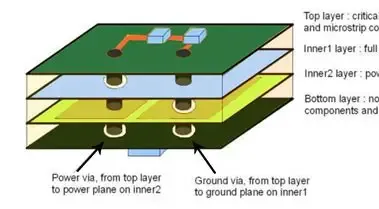
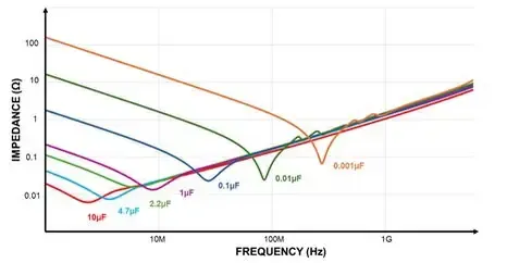
The power distribution network consists of voltage regulator modules, copper planes or traces, vias, and decoupling networks that collectively present a frequency-dependent impedance to the load. Target impedance is derived from the maximum allowable voltage ripple and the peak current demand of the circuitry, ensuring that the network impedance remains below this threshold across the frequency range of interest. At low frequencies, bulk capacitance from the battery and regulator output capacitors dominates, while mid-frequency behavior depends on the placement and values of ceramic decoupling capacitors. High-frequency impedance is governed by the inductance of vias, plane spreading, and the equivalent series inductance of the capacitors themselves. Simultaneous switching noise arises when multiple output drivers change state at the same time, inducing voltage spikes on the power and ground rails proportional to the total inductance of the current loop.
Power plane impedance optimization begins with minimizing the loop area between power and return paths. Solid copper planes provide lower inductance than routed traces, yet cutouts for signal routing or mounting holes can create localized high-impedance regions. Return path discontinuities force high-frequency currents to take longer routes, increasing both inductance and radiated emissions. Decoupling capacitor selection therefore balances capacitance value, voltage rating, package size, and parasitic inductance to create a broadband low-impedance path. Multiple capacitor values placed in parallel extend the effective frequency coverage because each value resonates at a different frequency determined by its parasitic inductance and the local plane capacitance.
Practical Solutions and Best Practices
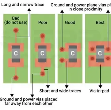
Engineers begin by establishing a target impedance profile based on the worst-case current transient and allowable ripple specified in component datasheets. Power planes are sized and layered to keep spreading inductance low, with stitching vias placed near high-current devices to maintain continuous return paths. Decoupling capacitors are located as close as possible to the power pins of integrated circuits, with the smallest value capacitors positioned nearest the die to address the highest frequencies. Via-in-pad or microvia constructions reduce the inductance between the capacitor and the plane, improving high-frequency performance. Simulation of the power distribution network using electromagnetic field solvers allows verification of impedance versus frequency before fabrication, revealing resonances that would otherwise require post-layout correction.
Additional measures include the use of embedded capacitance materials between power and ground planes when board thickness permits, providing distributed capacitance that lowers impedance without discrete components. Careful stack-up planning ensures that high-speed signals reference the nearest plane, reducing crosstalk into power nets. Thermal vias under power components help maintain lower operating temperatures, preserving capacitor performance over the product lifetime. Validation after assembly involves time-domain reflectometry or vector network analyzer measurements on test coupons to confirm that the fabricated board meets the simulated impedance targets.
Conclusion
Power integrity analysis forms an essential part of wearable PCB development because even small voltage deviations can compromise device reliability and user safety. Systematic attention to power distribution network design, combined with informed decoupling capacitor selection and simultaneous switching noise reduction techniques, yields stable voltage delivery across operating conditions. Power plane impedance optimization further ensures that the network presents low impedance from DC through the highest relevant frequencies. When these practices are applied consistently, wearable products achieve the performance and longevity expected in medical, fitness, and consumer markets.
FAQs
Q1: How does power distribution network design influence battery life in wearable devices?
A1: A well-optimized power distribution network reduces resistive and inductive losses between the battery and the load, allowing more of the stored energy to reach the active circuits rather than being dissipated as heat. Lower impedance also permits the voltage regulator to operate more efficiently across varying load currents, extending runtime between charges while maintaining stable voltage rails for all components.
Q2: What factors guide decoupling capacitor selection for high-density wearable PCBs?
A2: Decoupling capacitor selection considers the frequency content of the load current transients, the parasitic inductance of each capacitor package, and the available board area. Engineers choose combinations of values and placements that collectively keep the power distribution network impedance below the target across the spectrum of interest, preventing voltage droop during simultaneous switching events.
Q3: Why is simultaneous switching noise reduction critical in compact wearable electronics?
A3: Simultaneous switching noise reduction prevents voltage spikes on shared power and ground rails that can exceed the noise margins of nearby analog or radio-frequency circuits. In space-constrained wearables, where power and signal paths are in close proximity, uncontrolled noise can corrupt sensor data or disrupt wireless communication links essential to device function.
Q4: How does power plane impedance optimization improve overall system reliability?
A4: Power plane impedance optimization minimizes voltage variation under dynamic loads, ensuring that every integrated circuit receives voltage within its specified operating range. Consistent voltage levels reduce the likelihood of timing violations, data errors, and thermal stress, contributing to longer product life and fewer field failures in wearable applications.
References
IPC-6012E — Qualification and Performance Specification for Rigid Printed Boards. IPC, 2017
JEDEC J-STD-020E — Moisture/Reflow Sensitivity Classification. JEDEC, 2014
ISO 9001:2015 — Quality Management Systems. ISO, 2015


