 ALLPCB


Introduction
In high-speed PCB design, panelization combines multiple individual boards into a single array for efficient manufacturing and assembly. While this approach reduces costs and streamlines production, PCB panel size directly influences signal integrity, particularly in applications with fast rise times and high frequencies. Larger panels can introduce variations in processing that affect impedance control and noise levels across the array. Engineers must balance economy with performance by selecting appropriate panel dimensions and layouts. This article explores the interplay between PCB signal integrity panel size and key factors like warpage, crosstalk, and electromagnetic interference. By following established best practices, designers can maintain reliable high-speed signal transmission throughout the production process.
Understanding PCB Panelization and Its Relevance to Signal Integrity
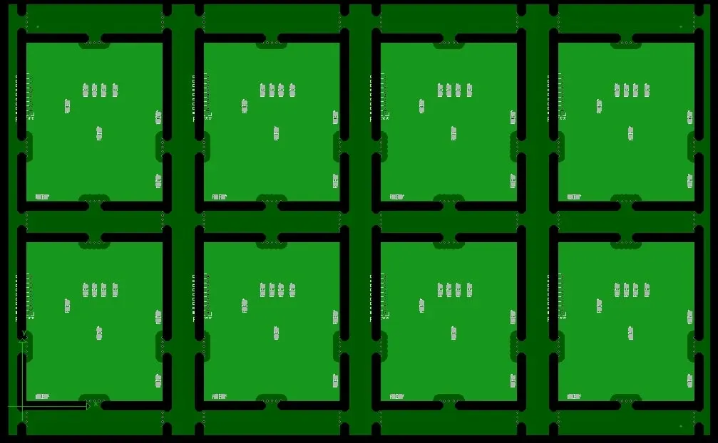
PCB panelization involves arranging multiple circuit boards on a larger carrier panel to optimize fabrication yields and assembly throughput. Common methods include V-scoring for straight-line separation and tab routing for irregular shapes. For high-speed designs, panelization must preserve signal quality, as manufacturing stresses can degrade performance. Signal integrity encompasses the preservation of electrical characteristics such as waveform shape, timing, and amplitude from transmitter to receiver. In panelized arrays, inconsistencies in etching, plating, or lamination across the panel can lead to variations in trace impedance and coupling between adjacent boards. These effects become critical as data rates exceed gigabit per second, where even minor deviations cause reflections or jitter.
Factory-driven insights emphasize that panel size dictates thermal uniformity during reflow soldering and lamination. Oversized panels experience greater temperature gradients, potentially warping the substrate and stressing high-speed traces. Adhering to IPC-2221 guidelines for printed board design helps mitigate these risks by promoting symmetric layouts and adequate border margins. Electrical engineers prioritize controlled impedance panel design to ensure consistent characteristic impedance across all boards in the array. Ultimately, thoughtful panelization supports high-speed PCB panelization without compromising end-product reliability.
Mechanisms Linking Panel Size to Signal Integrity Challenges
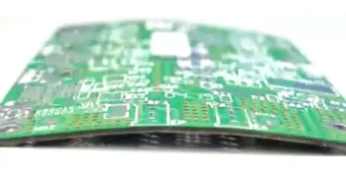
Panel size impacts signal integrity through several interconnected mechanisms rooted in material behavior and process variations. Larger panels amplify warpage due to asymmetric thermal expansion during lamination and baking cycles. This bowing alters the distance between trace layers, shifting the effective dielectric thickness and thus the controlled impedance of striplines or microstrips. In high-speed signals, such changes introduce mismatches that reflect energy back to the source, distorting eye diagrams.
Crosstalk arises when signals from one board couple into neighboring ones via capacitive or inductive mechanisms, exacerbated in dense panels with minimal spacing. Parallel traces running near panel edges or break lines pick up mutual inductance, especially if depaneling vibrations propagate mechanically. Noise coupling intensifies with panel size because longer exposure to process baths leads to uneven copper deposition, widening trace width tolerances. Reducing noise panel techniques, such as increasing inter-board gaps, become essential to isolate sensitive nets.
Electromagnetic interference considerations further complicate large panels. EMI panel considerations include radiation from panel edges where ground planes terminate abruptly, creating slot antennas. During high-speed operation, these discontinuities leak energy, failing emissions compliance. Additionally, via stub lengths vary across the panel due to drill wander in oversized arrays, attenuating signals or generating resonances. Understanding these principles guides engineers toward panel sizes that minimize variance while maximizing utilization.
Detailed Effects on Key Signal Integrity Parameters
Impedance control stands as a cornerstone of high-speed performance, yet panel size challenges its uniformity. Etching processes on expansive panels suffer from undercuts at the center versus edges due to spray patterns and developer flow. This results in trace geometries deviating from design intent, altering the Z0 for differential pairs critical in protocols like PCIe or DDR. Factory measurements using time-domain reflectometry reveal tolerances tightening to plus or minus 10 percent only on smaller panels.
Crosstalk noise scales with panel density and size. Near-end and far-end coupling increase when high-speed lines align across board boundaries without sufficient guard traces. Mechanical stresses from depaneling propagate as micro-cracks, intermittently shorting or opening nets. EMI escalates as panel perimeter grows, with unshielded edges acting as efficient radiators for harmonics above 1 GHz.
Power delivery integrity suffers indirectly, as larger panels demand thicker copper pours that bow under current, raising plane impedance. These effects compound in multilayer stacks, where interlayer alignment drifts. IPC-6012 specifications for rigid board qualification underscore the need for flatness control to prevent such anomalies during assembly.
Best Practices for High-Speed PCB Panelization
Select panel dimensions based on equipment capabilities and signal speed requirements, favoring compact arrays for gigahertz designs. Orient identical boards symmetrically around the panel center to equalize process exposure and minimize warpage gradients. Incorporate fiducial marks at corners and center for precise alignment during routing and inspection.
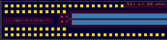
For controlled impedance panel design, position test coupons at multiple locations, including edges and center, to verify uniformity post-fabrication. Route high-speed traces inward from panel borders by at least 5 mm to avoid edge effects during scoring. Employ tab routing with perforated breaks on non-critical edges, ensuring no high-speed vias near fracture lines.
Reducing noise panel techniques include staggering board orientations to misalign parallel traces and adding ground stitching vias along inter-board gaps. Maintain minimum spacing of three times the trace width between arrays to suppress coupling. For EMI panel considerations, extend ground planes to panel edges with seamless pours and overlap return paths under signals.
Layer stackup symmetry aids flatness; use balanced cores and prepregs per IPC-6012. Simulate panel-level effects using field solvers to predict crosstalk before tape-out. During depaneling, opt for laser or waterjet methods over mechanical routing to reduce vibrations impacting delicate traces.
In assembly, support large panels with custom fixtures to prevent sagging in reflow ovens. Post-depaneling, inspect for microcracks via electrical testing. These practices ensure high-speed PCB panelization yields boards with robust signal integrity.
Troubleshooting Common Panelization Issues in High-Speed Designs
Engineers often encounter impedance drift in outer boards of large panels, traceable to uneven lamination pressure. Verify stackup drawings specify uniform cure cycles and measure Z0 across the array. Warpage exceeding 0.75 percent total indicator reading signals oversize panels; downsize or add stress-relief slots.
Crosstalk spikes near tabs indicate inadequate spacing; redesign with wider rails. EMI failures post-assembly point to incomplete ground flooding; audit copper balance. Use cross-talk budgets from simulation to set spacing rules early.
A factory case revealed a 400 mm panel causing 15 percent impedance variation in USB 3.0 traces. Switching to dual 200 mm panels with rotated layouts restored tolerances. Systematic root-cause analysis, aligned with J-STD-020 for handling, resolves most issues.
Conclusion
Optimizing PCB panel size is crucial for preserving signal integrity in high-speed applications. By addressing warpage, impedance variations, noise coupling, and EMI through strategic design and process controls, engineers achieve reliable performance. Symmetric layouts, adequate margins, and verification coupons form the backbone of effective high-speed PCB panelization. Implementing these best practices reduces risks and enhances yield. Electrical engineers benefit from factory insights emphasizing standard compliance for consistent outcomes.
FAQs
Q1: How does PCB signal integrity panel size affect high-speed designs?
A1: Larger panels introduce warpage and process non-uniformities that alter trace impedance and increase crosstalk between boards. Smaller panels ensure better thermal control and etching consistency, preserving waveform integrity for signals above 1 GHz. Always simulate panel-level effects and measure post-fabrication to confirm tolerances. This approach aligns with manufacturing realities for optimal results.
Q2: What are key elements of high-speed PCB panelization?
A2: High-speed PCB panelization requires symmetric board placement, fiducials for alignment, and wide borders around high-speed nets. Use tab routing away from signals and verify flatness to avoid stress-induced failures. Ground stitching along gaps reduces coupling. These steps maintain signal quality across the array during fabrication and assembly.
Q3: How to achieve controlled impedance panel design?
A3: Controlled impedance panel design involves placing test structures at panel quadrants and specifying tight fab tolerances. Symmetric stackups prevent dielectric variations, while edge avoidance for critical traces ensures uniformity. Post-etch TDR testing confirms Z0 consistency. This factory-aligned method supports reliable high-speed performance without redesigns.
Q4: What reducing noise panel techniques work best for EMI?
A4: Reducing noise panel techniques include inter-board ground planes, staggered trace routing, and EMI shielding vias. Extend returns under signals and minimize panel perimeter discontinuities. Laser depaneling cuts vibration-induced noise. EMI panel considerations like full copper floods comply with emissions needs in dense arrays.
References
IPC-2221B — Generic Standard on Printed Board Design. IPC, 2003
IPC-6012E — Qualification and Performance Specification for Rigid Printed Boards. IPC, 2015
J-STD-020E — Moisture/Reflow Sensitivity Classification for Nonhermetic Surface Mount Devices. JEDEC/IPC, 2014





