ALLPCB


Are you struggling with heat management in your PCB designs? One key factor often overlooked is copper weight. In PCB layout thermal design, copper weight plays a vital role in dissipating heat, ensuring reliability, and maintaining performance in electronic devices. In this detailed guide, we’ll explore why copper weight is crucial for thermal management and how to optimize your PCB layout for better heat dissipation.
Whether you’re designing for consumer electronics, automotive systems, or industrial applications, understanding the impact of copper weight can make or break your project. Let’s dive into the essentials of PCB thermal design and uncover actionable tips to enhance your designs.
What Is PCB Layout Thermal Design?
PCB layout thermal design focuses on managing heat generated by components on a printed circuit board. As electronic devices become smaller and more powerful, components like processors, power supplies, and LEDs produce significant heat. If not managed properly, this heat can lead to performance issues, reduced lifespan, or even complete failure of the device.
Thermal design involves several strategies, including material selection, component placement, and the use of copper layers. Copper, with its high thermal conductivity, acts as a primary pathway for heat to move away from hot components and spread across the board or into a heat sink. This is where copper weight—measured in ounces per square foot (oz/ft2)—becomes a critical factor.
Why Copper Weight Matters in Thermal Design
Copper weight refers to the thickness of the copper layer on a PCB, typically ranging from 0.5 oz/ft2 to 4 oz/ft2 or higher in specialized applications. A standard PCB often uses 1 oz/ft2, which translates to a thickness of about 35 micrometers. But why does this matter for thermal management?
Copper’s thermal conductivity is around 400 W/m·K, far higher than the FR4 substrate material commonly used in PCBs, which has a thermal conductivity of only about 0.3 W/m·K. This means copper can transfer heat much more effectively. A heavier copper weight provides a thicker and wider path for heat to travel, reducing thermal resistance and helping to keep components cool.
For example, in a high-power application like a motor controller, using a 2 oz/ft2 copper layer instead of 1 oz/ft2 can reduce the temperature rise by up to 20-30% under the same load, depending on the layout. This directly improves reliability and prevents thermal hotspots that could damage sensitive components.
How Copper Weight Impacts Heat Dissipation
The relationship between copper weight and heat dissipation is straightforward: thicker copper layers can carry more heat away from components. This is especially important in designs with high current demands, where heat generation is significant due to resistive losses (I2R losses).
Consider a power supply circuit delivering 10 amps through a trace. With a 1 oz/ft2 copper layer, the trace might experience a temperature rise of 50°C above ambient due to limited heat dissipation. By increasing the copper weight to 3 oz/ft2, the temperature rise could drop to 20-25°C, as the thicker copper spreads heat more effectively and reduces resistance.
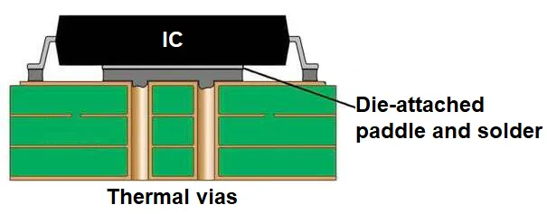
Additionally, heavier copper allows for wider traces and larger copper planes, which act as mini heat sinks. These planes can distribute heat across a larger area, lowering the overall thermal resistance of the board. In multi-layer PCBs, internal copper planes connected by thermal vias further enhance this effect by providing additional paths for heat to escape.
Choosing the Right Copper Weight for Your Design
Selecting the appropriate copper weight depends on several factors, including the application, current requirements, and space constraints. Here’s a breakdown of common copper weights and their typical uses in PCB layout thermal design:
- 0.5-1 oz/ft2: Suitable for low-power applications like consumer electronics with minimal heat generation. Commonly used in standard designs to keep costs low.
- 2 oz/ft2: Ideal for moderate power applications, such as LED lighting or small power supplies, where heat dissipation needs are higher but cost remains a concern.
- 3-4 oz/ft2 or higher: Used in high-power applications like automotive electronics, industrial equipment, and aerospace systems. These designs prioritize thermal performance and current-carrying capacity over cost.
Keep in mind that heavier copper increases material and manufacturing costs. It also affects the overall thickness of the PCB, which may be a concern in compact designs. Balancing thermal needs with budget and space constraints is essential.
Best Practices for Optimizing Copper in Thermal Design
While choosing the right copper weight is important, how you use it in your PCB layout is just as critical. Here are some practical tips to maximize thermal performance:
1. Use Copper Planes for Heat Spreading
Incorporate large copper planes on the top, bottom, or internal layers of your PCB. These planes act as heat spreaders, distributing thermal energy away from hot components. Connect these planes to ground or power nets for added functionality, ensuring they cover as much area as possible without interfering with signal integrity.
2. Add Thermal Vias
Thermal vias are small holes filled or plated with copper that connect copper layers vertically. Place them near high-heat components to transfer heat from the top layer to inner or bottom layers, where it can dissipate more effectively. For example, placing 10-15 thermal vias under a power IC can reduce its operating temperature by 10-15°C.
3. Optimize Trace Widths
For high-current traces, use wider paths to minimize resistance and heat buildup. A trace carrying 5 amps on a 1 oz/ft2 copper layer might need to be 100 mils wide to keep temperature rise below 10°C. Use online trace width calculators to determine the exact dimensions based on current and copper weight.
4. Balance Copper Distribution
Uneven copper distribution can cause mechanical stress and warping during manufacturing due to uneven heat dissipation. Ensure copper weight is balanced across layers (e.g., match the top and bottom layers) to maintain structural integrity and consistent thermal performance.
Challenges with Heavy Copper Weights
While heavier copper offers clear thermal benefits, it comes with challenges that designers must address:
- Cost: Heavier copper weights increase material and processing costs. For instance, moving from 1 oz/ft2 to 3 oz/ft2 can raise production costs by 20-30%, depending on the board size and complexity.
- Manufacturing Complexity: Thicker copper layers are harder to etch precisely, potentially leading to issues with fine traces or small features. This is a concern for high-density designs.
- Weight and Size: Heavier copper adds to the overall weight and thickness of the PCB, which may not be suitable for portable or space-constrained devices.
To mitigate these issues, consider hybrid designs where only specific areas of the PCB use heavier copper (e.g., around power components), while other sections use standard weights to save on cost and weight.
Thermal Simulation: Testing Your Design
Before finalizing your PCB layout, use thermal simulation software to predict heat distribution and identify potential hotspots. These tools analyze factors like copper weight, component placement, and airflow to estimate temperature rises under operating conditions.
For example, a simulation might reveal that a critical component reaches 85°C with a 1 oz/ft2 copper layer under a 5W load. By increasing to 2 oz/ft2 and adding thermal vias, the temperature might drop to 65°C, well within safe operating limits. Such insights allow you to adjust copper weight and layout early in the design process, saving time and cost during prototyping.
Real-World Applications of Copper Weight in Thermal Design
Let’s look at how copper weight impacts thermal design in specific industries:
Automotive Electronics
In electric vehicle (EV) battery management systems, high currents (often exceeding 20 amps) generate substantial heat. Using 3-4 oz/ft2 copper layers ensures efficient heat dissipation, preventing thermal runaway in battery packs. Large copper planes and thermal vias are often used to channel heat to external heat sinks.
LED Lighting
High-power LEDs can produce temperatures exceeding 100°C at the junction. A 2 oz/ft2 copper layer with a well-designed thermal pad can reduce junction temperature by 15-20°C, extending the LED’s lifespan and maintaining brightness.
Industrial Power Supplies
Industrial systems often operate in harsh environments with limited airflow. Heavy copper weights (4 oz/ft2 or more) are critical to handle high power loads and ensure reliable operation, even at elevated ambient temperatures.
Conclusion: Prioritize Copper Weight in Your PCB Thermal Design
In PCB layout thermal design, copper weight is a cornerstone of effective heat management. By selecting the right copper thickness and optimizing your layout with planes, vias, and balanced distribution, you can significantly improve the thermal performance of your designs. While heavier copper comes with challenges like cost and manufacturing complexity, the benefits in reliability and longevity often outweigh the drawbacks, especially in high-power applications.
Start by evaluating the thermal needs of your project and experimenting with different copper weights during the design phase. Use simulation tools to validate your choices and ensure your PCB can handle the heat. With the right approach, you’ll create designs that not only perform well but also stand the test of time.
At ALLPCB, we’re committed to helping you achieve optimal thermal performance in your PCB designs. Whether you’re working on a simple prototype or a complex industrial system, our expertise and resources are here to support your success.