 ALLPCB


Introduction
Wave soldering remains a reliable process for attaching through-hole components to printed circuit boards in high-volume production environments. Engineers focus on panel size because it directly influences process stability, defect rates, and overall manufacturing efficiency. Proper panel dimensions allow consistent solder wave contact, reduce thermal stress, and support automated handling systems. When panel size is optimized, manufacturers achieve higher yields while maintaining compliance with established quality requirements. This guide outlines the engineering considerations and practical steps for achieving effective results.
Why PCB Panel Size Matters in the Wave Soldering Process
Panel size selection affects multiple aspects of the wave soldering process, including thermal distribution and mechanical support during conveyor transport. Oversized panels can lead to excessive warpage under heat, while undersized panels may reduce throughput and increase per-unit handling costs. The design must accommodate support rails, fiducials, and breakaway tabs without interfering with component placement or solder flow. Industry experience shows that balanced panel dimensions improve solder joint consistency across through-hole leads and minimize bridging or icicle formation. Attention to these factors supports repeatable outcomes in mixed-technology assemblies that combine surface-mount and through-hole parts.
Technical Principles of Wave Soldering Panel Design
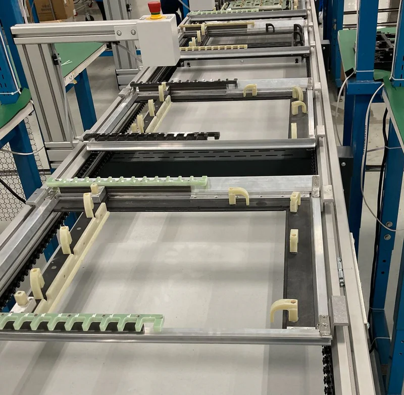
The wave soldering process exposes the board to a controlled solder wave that must wet component leads uniformly while avoiding excess heat on sensitive areas. Panel size influences thermal mass, which in turn affects preheat profiles and cooling rates. Larger panels require careful zoning to prevent localized overheating, whereas smaller panels may cool too quickly and produce incomplete joints. Warpage control becomes critical because uneven expansion can lift leads out of the wave or cause misalignment. Standards such as IPC-6012E provide qualification criteria for rigid boards that help engineers evaluate material and construction choices before panelization. Component orientation also plays a role, as leads must align parallel to the direction of travel to ensure proper solder fillet formation.
Step-by-Step Guide to Optimizing Panel Size
Begin by reviewing the wave soldering equipment specifications for maximum and minimum panel dimensions that the conveyor and wave nozzle can accommodate. Next, map component locations to ensure adequate spacing from panel edges and between rows so that the solder wave contacts all leads without shadowing. Add support rails or breakaway sections along the longer edges to maintain rigidity during transport and reduce flexing. Incorporate fiducial marks and tooling holes at standardized positions that align with the machine vision system. Finally, simulate or prototype the panel layout to verify solder coverage and inspect for defects before committing to full production runs. This structured approach helps balance throughput goals with quality targets.
Best Practices for PCB Panel Design in Through-Hole Applications
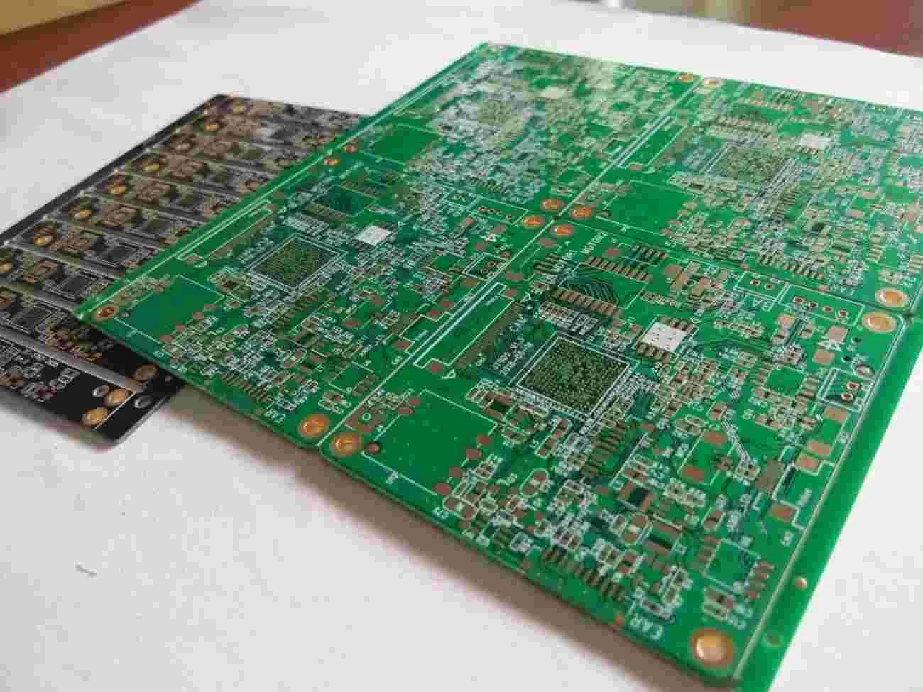
Designers should maintain consistent panel thickness and copper distribution to limit warpage during the thermal cycle. Place heavier through-hole components toward the center of the panel where support is greatest, and avoid clustering leads near the edges that contact the wave first. Use appropriate solder mask and surface finishes that promote wetting without excessive dross accumulation. When multiple boards share a panel, ensure that scoring or routing lines do not compromise structural integrity during handling. Regular process monitoring, including visual inspection of solder joints, helps identify when panel adjustments are needed. These practices align with broader quality expectations outlined in IPC-A-600K for board acceptability.
Conclusion
Optimizing PCB panel size for wave soldering requires attention to equipment limits, thermal behavior, and component layout. A logical, step-wise evaluation of these elements supports consistent joint quality and efficient production. By applying established engineering principles and referencing relevant industry standards, teams can reduce defects while meeting throughput requirements. Continued process refinement based on measured results further strengthens manufacturing outcomes over time.
FAQs
Q1: What factors determine the best PCB panel size for wave soldering?
A1: Panel size selection depends on equipment conveyor limits, component density, and the need to control warpage during the thermal cycle. Engineers evaluate support rail placement and fiducial positioning to ensure stable transport and uniform solder contact. Proper sizing also supports efficient throughput without compromising joint quality on through-hole components.
Q2: How does wave soldering panel design influence through-hole component reliability?
A2: Panel design affects lead alignment with the solder wave and the amount of thermal stress applied to each joint. Consistent panel dimensions reduce flexing that could lift leads or create insufficient solder. Attention to spacing and orientation helps achieve reliable fillets that meet acceptance criteria.
Q3: What steps help optimize panel layout for the wave soldering process?
A3: Start with equipment specifications, then arrange components to avoid shadowing and place support features along the edges. Add fiducials and verify the layout through prototyping before production. These actions promote repeatable results across batches.
Q4: Why is panel size important when mixing surface-mount and through-hole components?
A4: Mixed-technology boards require panel dimensions that accommodate both reflow and wave processes without excessive handling. Balanced sizing prevents warpage that could affect fine-pitch surface-mount parts while still allowing full wave coverage of through-hole leads.





