 ALLPCB


Introduction
Electromagnetic compatibility (EMC) ensures that electronic devices operate without causing or suffering undue electromagnetic interference (EMI). In printed circuit board (PCB) design, layer stackup defines the sequence of copper layers, power planes, ground planes, and insulating materials, directly influencing EMI performance. Poorly optimized stackups amplify radiated and conducted emissions, complicating EMC compliance testing. Engineers must prioritize PCB layer stackup for EMI control from the initial design phase to minimize costly redesigns. This practical guide outlines structured approaches grounded in PCB design rules, focusing on shielding techniques and layer arrangements that promote low-impedance return paths and effective field containment. By following these strategies, designers achieve robust EMC performance across various board complexities.
Understanding PCB Layer Stackup and Its Role in EMI/EMC
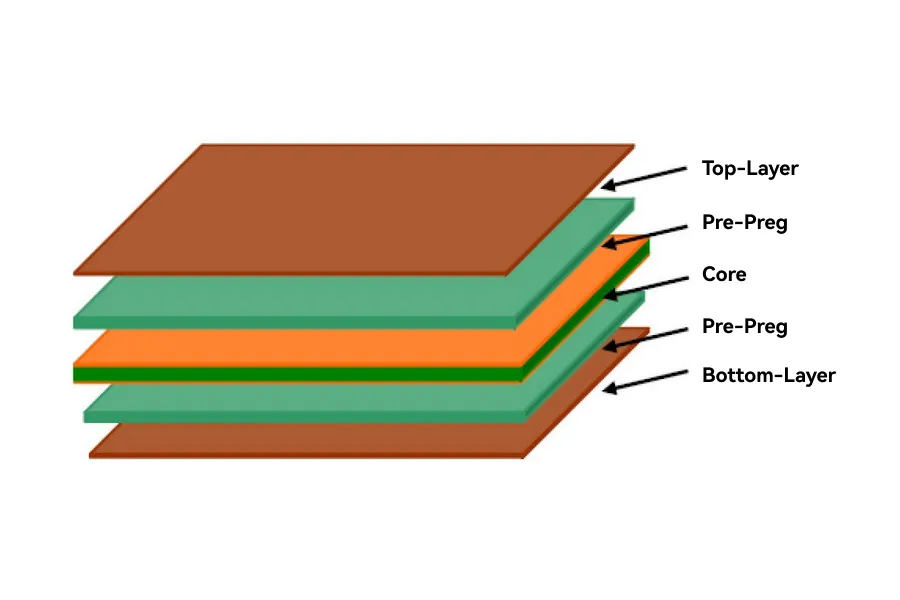
PCB layer stackup refers to the vertical arrangement of conductive layers separated by dielectric cores and prepregs, determining electrical, thermal, and mechanical properties. For EMI management, stackup controls signal propagation modes, such as microstrip on outer layers or stripline internally, which affect impedance and radiation. A well-planned stackup provides continuous reference planes that serve as shields, reducing loop areas where currents can radiate electromagnetic fields. Electromagnetic interference arises from unintended coupling between traces or planes, leading to crosstalk or external emissions that violate EMC limits. Optimizing PCB layer stackup for EMI thus aligns with core PCB design rules, ensuring predictable signal behavior and compliance. This foundation enables engineers to balance routing density with emission control.
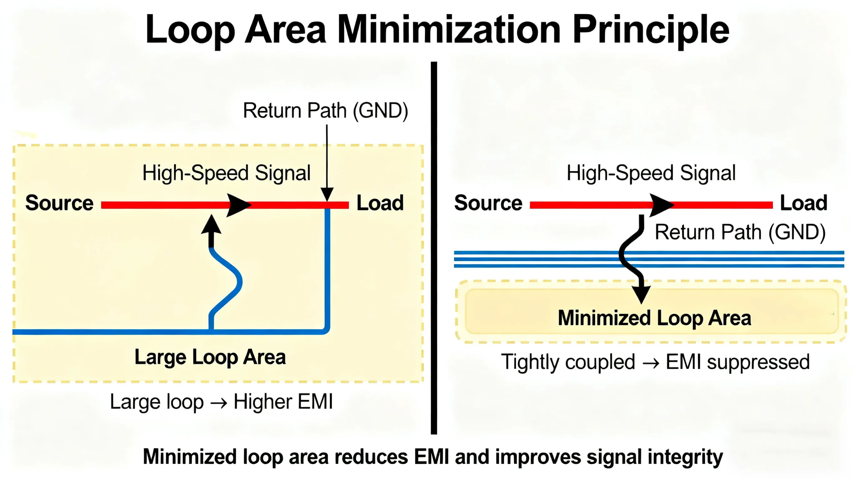
In high-speed designs, stackup influences common-mode and differential-mode currents, where unbalanced returns exacerbate EMI. Ground planes adjacent to signal layers shorten return paths, minimizing inductance and radiated fields. Power distribution layers, when paired closely with grounds, form distributed capacitors that suppress noise. These configurations directly support EMC compliance by confining fields within the board structure.
Key Principles of EMI Generation and Propagation in PCBs
EMI in PCBs stems from time-varying electric and magnetic fields generated by switching currents in traces and components. Radiated EMI occurs when current loops act as antennas, with efficiency peaking at wavelengths matching loop dimensions. Conducted EMI travels through power lines or cables, often amplified by poor plane partitioning. Layer stackup mitigates these by providing low-inductance paths that force return currents to mirror forward paths closely, reducing net loop areas. Shielding techniques, such as broad ground pours, reflect or absorb fields, preventing propagation to sensitive areas or outside the enclosure.
Magnetic fields dominate near-field coupling, penetrating dielectrics easily, while electric fields are more contained by planes. In multilayer boards, splitting planes without stitching vias creates slits that radiate like slots. PCB design rules emphasize plane continuity and via fencing to maintain shielding effectiveness. Understanding these mechanisms guides stackup decisions, ensuring fields decay rapidly away from sources. IPC-2221B outlines principles for layer spacing and impedance control that indirectly bolster EMI suppression through consistent field management.
Best Practices for Optimizing Layer Stackup
Start with the simplest effective stackup: for 4-layer boards, place signal layers on top and bottom, with inner layers dedicated to ground and power. This configuration sandwiches signals between planes, achieving stripline-like isolation on outer layers via tight coupling. Maintain thin dielectrics between power and ground planes, ideally under 0.2 mm, to leverage capacitive decoupling and reduce impedance. Avoid placing high-speed signals on adjacent layers without intervening planes, as this invites broadside coupling. Route sensitive traces parallel to plane edges, minimizing perpendicular crossings that induce noise.
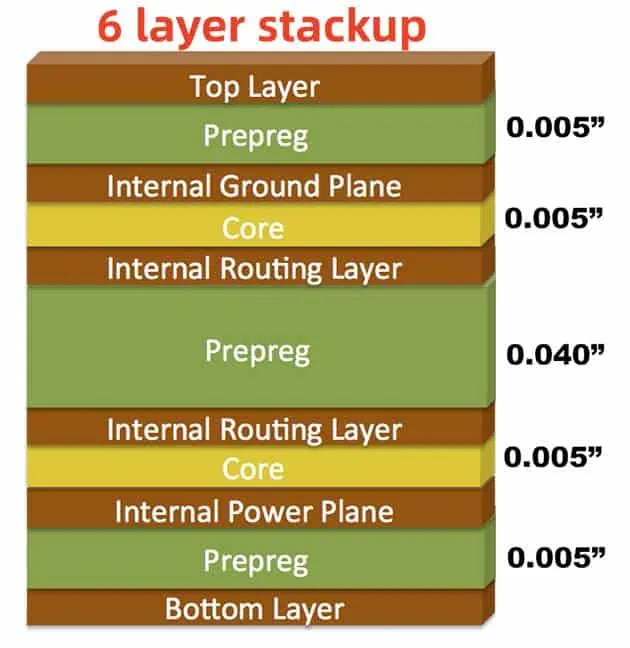
For 6-layer boards, expand to signal-ground-signal-power-signal-ground, providing dual reference planes per signal layer. This enhances shielding techniques by distributing return paths, crucial for mixed-signal designs. Power planes should interleave with grounds to form multiple decoupling pairs, suppressing ripple currents that contribute to EMI. Symmetry in core and prepreg thicknesses prevents warpage, maintaining consistent dielectric distances for impedance stability. Adhere to PCB design rules for minimum layer spacing to avoid fringing fields.
In 8-layer or higher stackups, alternate signal and plane layers rigorously, dedicating at least 40% of layers to planes. Core high-speed signals internally between planes for maximum containment. Use split planes judiciously, stitching edges with dense via arrays to block slot radiation. These practices form the backbone of PCB layer stackup for EMI optimization, ensuring EMC compliance across frequencies.
Advanced Shielding Techniques in Layer Stackup
Shielding techniques extend beyond basic planes through guard traces, moats, and via walls that compartmentalize noise. In stackup planning, align ground pours across multiple layers, connected by through-vias every few millimeters, to create Faraday cage-like barriers. For mixed-signal boards, dedicate isolated ground planes per analog and digital sections, bridged only at single points to prevent ground bounce propagation. Controlled impedance traces, matched to 50 or 100 ohms per IPC-2221B guidelines, reduce reflections that broaden emission spectra.
Consider dielectric constants: lower-loss materials in high-frequency stackups minimize absorption losses while maintaining field confinement. Prepreg selection influences coupling strength, with thinner sheets enhancing plane capacitance. Simulate stackup parasitics early to predict EMI hotspots, adjusting layer order iteratively. These refinements elevate basic stackups to production-ready designs compliant with EMC requirements.
Troubleshooting Stackup-Related EMI Issues
Excessive emissions often trace to distant signal-plane pairings, where fields fringe outward. Measure near-field probes during prototyping to identify radiating loops, then insert ground planes or reroute accordingly. Crosstalk spikes indicate insufficient layer separation; tighten coupling or add shielding planes. Plane splits without vias manifest as conducted EMI peaks; remedy with stitching grids. Warped boards from asymmetric stackups alter clearances, worsening coupling; balance thicknesses per manufacturing specs.
Post-layout reviews verify plane utilization over 70% to avoid resonance. EMC pre-compliance scans guide stackup tweaks before formal testing. Consistent application of these diagnostics ensures robust PCB layer stackup for EMI control.
Conclusion
Optimizing PCB layer stackup demands a systematic focus on plane adjacency, impedance control, and shielding techniques to curb electromagnetic interference. From 4-layer basics to multilayer complexities, these PCB design rules deliver EMC compliance reliably. Engineers benefit from early integration of ground references and symmetric builds, minimizing redesign cycles. Practical adherence yields quieter boards with superior signal integrity. Prioritize stackup as the cornerstone of EMI-resilient designs.
FAQs
Q1: What are the primary PCB design rules for layer stackup to achieve EMC compliance?
A1: Key rules include placing signal layers adjacent to continuous ground or power planes, maintaining thin dielectrics between power and ground for decoupling, and ensuring plane symmetry to avoid warpage. Dense via stitching at splits prevents radiation. These practices, aligned with standards like IPC-2221B, reduce loop areas and field coupling, facilitating passage of EMC tests without extensive shielding add-ons.
Q2: How does PCB layer stackup for EMI reduction differ in 4-layer versus 6-layer boards?
A2: In 4-layer boards, top/bottom signals flank inner ground/power planes for basic shielding. 6-layer expands with additional signal layers interleaved between planes, offering dual references and better isolation for high-speed signals. This progression enhances electromagnetic interference containment while supporting denser routing, critical for EMC compliance in complex designs.
Q3: What shielding techniques improve EMI performance in multilayer stackups?
A3: Effective techniques involve via fences around noisy areas, guard rings on signal layers, and overlapping ground pours across planes. Interleaving power/ground pairs forms distributed capacitors to shunt noise. These methods, combined with controlled impedance traces, minimize emissions and crosstalk, ensuring robust PCB layer stackup for EMI control per established design principles.
Q4: Why is plane adjacency crucial for electromagnetic interference mitigation?
A4: Adjacent planes provide low-inductance return paths, confining magnetic fields and reducing radiation efficiency. Without adjacency, signals propagate as microstrips with broader fields prone to coupling. This principle underpins PCB design rules for EMC compliance, enabling shielding techniques that pass regulatory limits reliably.
References
IPC-2221B — Generic Standard on Printed Board Design. IPC, 2012
IPC-6012E — Qualification and Performance Specification for Rigid Printed Boards. IPC, 2020
IEC/TR 61000-5-2 — Electromagnetic compatibility (EMC) — Part 5-2: Installation and mitigation guidelines — Earthing and cabling. IEC, 1997





