 ALLPCB


Introduction
Mouse bites provide a practical method for separating individual printed circuit boards from larger panels after fabrication and assembly. Hobbyists and small-scale designers often work with panelized boards to simplify handling during manufacturing and testing. These breakaway features consist of small perforations arranged along designated tabs that connect the boards within the panel. When designed correctly, they allow clean separation without specialized equipment while minimizing the risk of damage to traces or components. Understanding their use supports efficient PCB panel creation and helps maintain board integrity throughout the process.
What Are Mouse Bites and Why They Matter
Mouse bites refer to patterns of small holes drilled or routed into breakaway tabs that link multiple PCBs in a single panel. This approach supports PCB panel creation by keeping boards stable during automated assembly steps such as solder paste application and component placement. For hobbyists, the technique reduces handling of fragile individual boards and lowers the chance of warping or cracking during transport. Proper implementation of creating breakaway tabs also aligns with quality expectations outlined in industry standards for rigid printed boards. The result is a more manageable workflow from design through final separation.
Technical Principles of Mouse Bite Design
The mechanism relies on controlled material removal that weakens the connection between boards just enough for manual or simple tool-assisted separation. Engineers arrange the perforations in a repeating pattern along the tab edges so that stress concentrates at the remaining material bridges. This design distributes forces evenly during depaneling and helps prevent jagged edges or lifted copper. Spacing and hole size influence the force required for separation as well as the cleanliness of the resulting edge. When integrated into overall panel layout, these features must account for the mechanical properties of the substrate to avoid unintended flexing or stress on nearby circuits. Industry guidelines such as those in IPC-6012E emphasize consistent fabrication practices that support reliable performance of such panel features.
How to Design Mouse Bites in PCB
Begin by defining the panel outline and identifying which boards will share edges that require breakaway tabs. Place the tabs at regular intervals along the shared boundaries while leaving sufficient clearance from active circuitry and mounting holes. Next, create the perforation pattern by specifying a series of small holes or slots that run perpendicular to the tab length. Adjust the number and arrangement of these features so the remaining material provides adequate strength during assembly yet yields cleanly when separation is needed. Review the full panel for mechanical balance to prevent distortion under thermal or handling loads. Finally, generate manufacturing files that clearly communicate the tab geometry and hole positions to the fabricator. This structured approach to how to design mouse bites in PCB supports repeatable results across multiple projects.
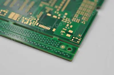
Best Practices for Creating Breakaway Tabs and PCB Panel Creation
Maintain consistent tab width and perforation density across the panel to ensure uniform separation force. Position tabs away from high-density component areas and sensitive signal paths to reduce the risk of damage during breaking. Consider adding small relief cuts or scoring at the tab ends to guide the separation line and improve edge quality. Verify that the overall panel dimensions and tab placement comply with handling requirements for both fabrication and assembly equipment. Test separation on a prototype panel before committing to larger production runs. These practices contribute to higher yield and fewer defects when following established acceptability criteria such as those detailed in IPC-A-600K.
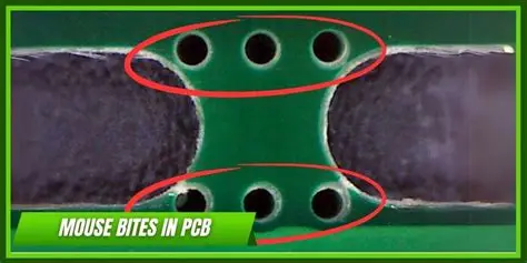
Troubleshooting Common Issues in Mouse Bite Implementation
Uneven separation often results from inconsistent hole spacing or insufficient tab strength. Review the perforation layout and adjust the remaining bridge width if boards require excessive force to detach. Chipped edges or lifted copper typically indicate that holes are positioned too close to traces or that the substrate experiences localized stress. Increasing clearance or modifying the pattern density can mitigate these effects. Warpage during assembly may stem from unbalanced tab placement that alters panel stiffness. Redistributing tabs more evenly or adding temporary support features helps maintain flatness. Systematic inspection after each prototype run identifies issues early and refines the design for subsequent iterations.
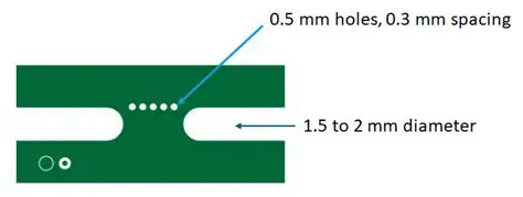
Conclusion
Mouse bites offer hobbyists an accessible way to manage PCB panel creation and achieve reliable separation of individual boards. Thoughtful application of design principles and adherence to recognized standards produces panels that withstand assembly processes while allowing clean breakaway. Consistent attention to tab geometry, perforation patterns, and clearance requirements supports both mechanical integrity and manufacturing efficiency. By following these guidelines, designers can incorporate creating breakaway tabs effectively into their workflows and improve overall project outcomes.
FAQs
Q1: How do I start learning how to design mouse bites in PCB layouts?
A1: Begin with basic panel outlines that group multiple boards logically. Define tab locations along shared edges and introduce simple perforation patterns that balance strength and ease of separation. Iterate on prototypes while checking for clean edges and minimal stress on circuitry. This mouse bites tutorial approach builds familiarity through repeated practical application.
Q2: What factors should I consider during PCB panel creation with breakaway tabs?
A2: Account for board thickness, component placement density, and the mechanical requirements of assembly steps. Ensure tabs provide enough rigidity for handling yet separate without damaging traces or pads. Consistent spacing and clearance from critical areas help maintain quality throughout fabrication and depaneling.
Q3: Can mouse bites tutorial guidance help avoid common depaneling problems?
A3: Yes, structured guidance emphasizes proper hole arrangement and tab sizing to control separation force. Reviewing designs against acceptability standards reduces risks such as jagged edges or component stress. Testing separation methods on sample panels further refines the approach before full production.
Q4: How does creating breakaway tabs fit into overall hobbyist PCB projects?
A4: Breakaway tabs integrate into panel designs to simplify handling of multiple boards during soldering and testing. They allow hobbyists to process several units efficiently while preserving individual board functionality after separation. Careful planning of tab features supports both small-batch builds and learning exercises in PCB design.
References
IPC-6012E — Qualification and Performance Specification for Rigid Printed Boards. IPC, 2017
IPC-A-600K — Acceptability of Printed Boards. IPC, 2020





