 ALLPCB


In the fast-evolving world of printed circuit board (PCB) design, microvias have become a game-changer, especially for high-density interconnect (HDI) applications. If you're looking to understand laser drilling microvias HDI PCBs, microvia design rules, or how to optimize laser drilling parameters for microvias, you've come to the right place. This guide dives deep into the essentials of PCB laser drilling, offering practical insights and actionable tips to help you master microvias for your next project.
At its core, laser drilling is a precise method used to create tiny holes, known as microvias, in PCBs. These microvias enable connections between layers in multilayer boards, saving space and improving performance in compact designs. Whether you're a PCB designer or an engineer, this comprehensive guide will walk you through everything from the basics to advanced techniques like microvia aspect ratio laser drilling and optimizing microvia laser drilling.
What Are Microvias and Why Do They Matter in HDI PCBs?
Microvias are small vias, typically less than 150 microns in diameter, used to connect different layers of a PCB. Unlike traditional through-hole vias that go through the entire board, microvias connect only specific layers, making them ideal for HDI PCBs where space is limited. They are often created using laser drilling, a non-contact method that ensures precision and minimizes damage to the board.
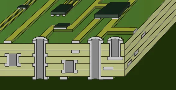
In HDI designs, microvias play a critical role. They allow for finer routing, reduced board size, and improved signal integrity by shortening the connection paths. For instance, in modern smartphones or wearable devices, where components are packed tightly, microvias help achieve high performance without increasing the footprint. Their ability to support fine-pitch components, like ball grid arrays (BGAs), also makes them indispensable in cutting-edge electronics.
The Basics of Laser Drilling for Microvias
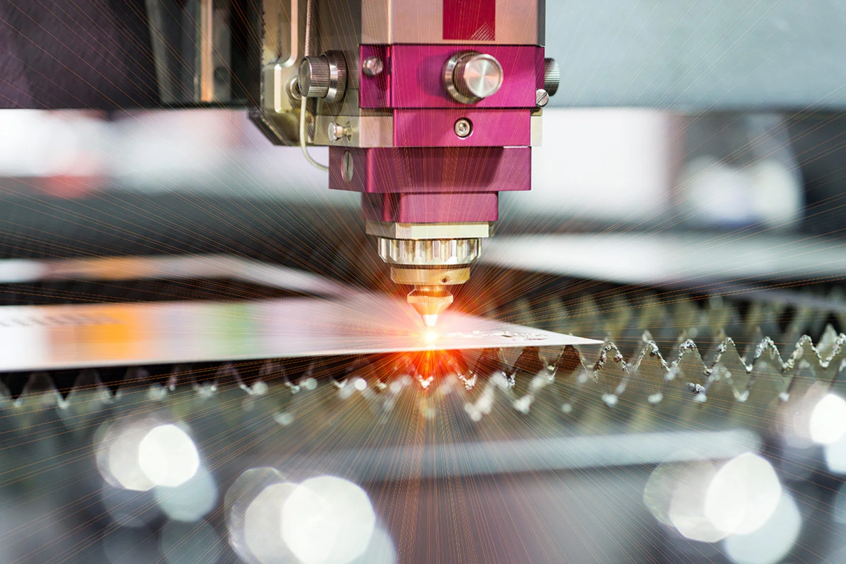
Laser drilling is the go-to technology for creating microvias due to its accuracy and ability to handle delicate materials. Unlike mechanical drilling, which can cause stress or damage to thin PCB layers, laser drilling uses a focused beam to vaporize material precisely where the via is needed. This process is especially effective for drilling holes with diameters as small as 50 microns.
The process works by directing a laser beam onto the PCB surface, typically using ultraviolet (UV) or carbon dioxide (CO2) lasers. UV lasers are preferred for their ability to drill through both copper and dielectric materials with minimal heat damage. The result is a clean, tapered hole that can be plated with copper to form an electrical connection between layers.
Laser drilling offers several advantages:
- Precision: Achieves hole sizes and placements with tolerances as tight as ±10 microns.
- Speed: Drills thousands of microvias per minute, ideal for high-volume production.
- Versatility: Works on various materials, including FR-4, polyimide, and high-frequency laminates.
Understanding Microvia Design Rules for Reliable PCBs
Designing microvias requires adherence to specific rules to ensure reliability and manufacturability. Ignoring these microvia design rules can lead to issues like poor plating, signal loss, or even board failure. Here are the key guidelines to follow:
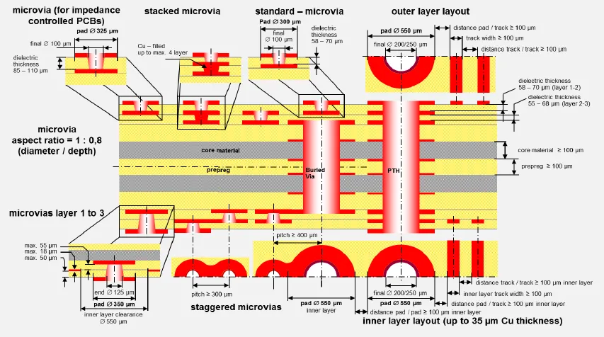
- Diameter and Depth: Microvias typically range from 50 to 150 microns in diameter. Their depth should not exceed 100-150 microns to maintain plating quality.
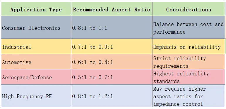
- Aspect Ratio: The aspect ratio (depth-to-diameter) of a microvia should ideally be 1:1 or less. Higher ratios, such as 1.2:1, can lead to incomplete copper plating and reliability issues during thermal cycling.
- Pad Size: The capture pad (the copper area surrounding the microvia) should be at least 50-75 microns larger than the via diameter to ensure proper alignment and connection.
- Spacing: Maintain a minimum spacing of 100 microns between microvias to avoid interference or structural weakness in the board.
- Stacking Limits: Stacked microvias (vias placed directly on top of each other across multiple layers) should not exceed two or three layers to prevent stress buildup.
Following these rules helps balance performance with manufacturing feasibility. For instance, a microvia with a 100-micron diameter and 100-micron depth maintains a 1:1 aspect ratio, ensuring uniform copper deposition during plating and reducing the risk of voids.
Key Laser Drilling Parameters for Microvias
The success of laser drilling depends on fine-tuning several parameters to match the material and design requirements. Adjusting these laser drilling parameters for microvias ensures clean holes, minimal thermal damage, and consistent results. Here are the critical factors to consider:
- Laser Power: Power levels typically range from 5 to 20 watts for UV lasers. Higher power can drill faster but risks burning the material, while lower power may result in incomplete holes.
- Pulse Duration: Short pulses (in the range of nanoseconds) reduce heat buildup, preventing damage to surrounding areas. Pulse durations of 10-50 nanoseconds are common for microvia drilling.
- Beam Focus: A tightly focused beam, often 20-50 microns in diameter, ensures precision. Misaligned focus can lead to uneven or oversized holes.
- Repetition Rate: The frequency of laser pulses, measured in kHz, affects drilling speed. Rates between 50-100 kHz are often used for a balance of speed and control.
- Material Type: Different substrates, like standard FR-4 or high-Tg materials, require tailored settings. For example, high-Tg laminates may need slightly higher power due to their denser composition.
By optimizing these parameters, manufacturers can achieve microvias with smooth walls and minimal debris, which is essential for reliable copper plating and signal transmission. For example, drilling a 75-micron via in a 0.1 mm thick dielectric layer might use a 10-watt UV laser with a 20-nanosecond pulse duration to avoid overheating.
Microvia Aspect Ratio in Laser Drilling: Why It Matters
The aspect ratio of a microvia, defined as the ratio of its depth to its diameter, is a critical factor in microvia aspect ratio laser drilling. A lower aspect ratio (closer to 1:1) is preferred because it allows for better copper plating and reduces the risk of defects. High aspect ratios, such as 2:1, can result in uneven plating, where the bottom of the via lacks sufficient copper, leading to weak connections.
Laser drilling excels at creating microvias with controlled aspect ratios. For instance, a microvia with a 100-micron diameter and 80-micron depth has an aspect ratio of 0.8:1, which is ideal for most HDI applications. However, achieving such precision requires careful calibration of laser parameters and material selection. Thin dielectric layers (less than 0.1 mm) are often used to keep the depth low and maintain a favorable ratio.
Challenges arise when drilling microvias with high aspect ratios. The deeper the hole relative to its diameter, the harder it is for the laser to remove material uniformly. This can lead to a phenomenon called "barrel distortion," where the via walls are not straight, impacting reliability. To address this, designers often limit microvia depth or use sequential lamination to build up layers gradually.
Optimizing Microvia Laser Drilling for Better Results
Optimizing microvia laser drilling is essential for achieving high-quality HDI PCBs that meet performance and reliability standards. Here are proven strategies to enhance the process:
- Material Selection: Choose dielectric materials with low laser absorption and high thermal stability to minimize damage. Thin layers (0.05-0.1 mm) also help maintain favorable aspect ratios.
- Layer-by-Layer Drilling: For multilayer boards, drill microvias after each lamination step rather than attempting to drill through multiple layers at once. This approach, known as sequential build-up, improves accuracy.
- Calibration and Testing: Regularly calibrate laser equipment to ensure consistent beam focus and power output. Test drilling on sample boards can help fine-tune parameters before full production.
- Cleaning Post-Drilling: After drilling, use a desmearing process to remove residue from via walls. This step ensures better copper adhesion during plating, reducing the risk of open circuits.
- Design for Manufacturability (DFM): Work closely with your manufacturing team to align design rules with their laser drilling capabilities. For example, avoid placing microvias too close to each other to prevent structural issues.
By focusing on these optimization techniques, you can reduce defects and improve the overall performance of your PCBs. For instance, a well-optimized process might achieve a drilling yield of over 99%, even for complex HDI designs with thousands of microvias.
Common Challenges in Laser Drilling Microvias and How to Overcome Them
Despite its precision, laser drilling microvias comes with challenges that can impact quality. Here are some common issues and solutions:
- Thermal Damage: Excessive heat from the laser can burn or delaminate the PCB material. Use lower power settings and shorter pulse durations to minimize heat buildup.
- Via Wall Roughness: Rough via walls can hinder copper plating. Adjust the laser focus and repetition rate to achieve smoother walls, and follow up with a chemical desmearing process.
- Alignment Errors: Misalignment can result in microvias that don’t connect properly. Use advanced imaging systems to ensure precise positioning during drilling.
- High Aspect Ratio Issues: As mentioned earlier, high aspect ratios lead to plating problems. Limit via depth or use stacked microvias across fewer layers to maintain a manageable ratio.
Addressing these challenges upfront can save time and cost in production, ensuring that your HDI PCBs perform reliably in real-world applications.
The Future of Microvia Laser Drilling in PCB Design
As electronics continue to shrink and demand higher performance, the role of microvias and laser drilling will only grow. Emerging trends include the use of ultra-thin materials (less than 0.05 mm) for even smaller microvias, as well as advancements in laser technology for faster and more precise drilling. Innovations like femtosecond lasers, which use ultra-short pulses, are also gaining traction for their ability to drill with virtually no heat damage.
Additionally, the rise of 5G, IoT, and automotive electronics is pushing the boundaries of HDI design. Microvias will be critical for supporting high-frequency signals (up to 28 GHz and beyond) with minimal loss, making laser drilling a cornerstone of future PCB manufacturing.
Conclusion: Elevate Your PCB Designs with Microvia Mastery
Mastering microvias through laser drilling is a powerful way to enhance your HDI PCB designs. By understanding laser drilling microvias HDI PCBs, adhering to microvia design rules, fine-tuning laser drilling parameters for microvias, managing microvia aspect ratio laser drilling, and focusing on optimizing microvia laser drilling, you can create compact, high-performance boards that meet the demands of modern electronics.
Whether you're working on consumer gadgets, medical devices, or industrial systems, the insights in this guide provide a solid foundation for success. With the right approach, microvias can unlock new possibilities in your PCB projects, delivering reliability and efficiency in even the most complex designs.


