 ALLPCB


Why PCB Dimensions Matter for Hobbyists
Board size directly affects how easily a design fits into an enclosure, how many components can be placed, and how the finished board behaves during soldering and use. Oversized boards increase the risk of warpage, handling damage, and higher fabrication expenses. Undersized boards may force cramped layouts that complicate routing or thermal management. Standard PCB sizes often align with common panel formats used by manufacturers, allowing multiple boards to be produced together efficiently. Hobbyists who respect these practical limits typically experience smoother ordering and better first-pass success.
Factors That Determine Maximum PCB Size
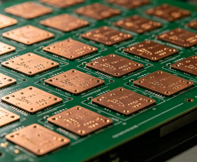
Several engineering considerations set practical upper bounds on board dimensions. Substrate materials expand and contract with temperature and moisture changes, and larger areas amplify any mismatch that leads to bowing or twisting. IPC standards address these material and performance requirements to maintain board integrity. Equipment such as imaging, etching, and drilling systems also has finite working areas, while handling large thin panels without flexing becomes more difficult. Designers therefore balance desired functionality against these physical realities from the start of a project.
Industry Standards That Guide Size and Quality
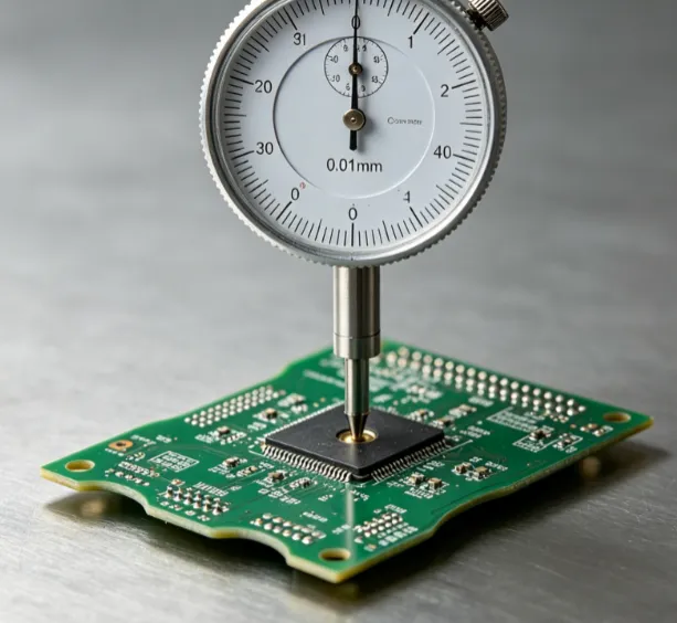
Quality specifications help define acceptable limits for size-related defects. IPC-6012E outlines qualification and performance requirements for rigid printed boards, including criteria that indirectly influence maximum usable dimensions. IPC-A-600K provides visual acceptance standards that cover issues such as warpage and twist on boards of various sizes. These documents emphasize consistent manufacturing practices rather than prescribing one maximum size for all applications. Hobbyists benefit from reviewing these guidelines when preparing files, as they highlight the measurements fabricators will verify.
Best Practices for Choosing and Ordering DIY PCB Sizes
Begin by sketching the circuit and estimating component placement before committing to final dimensions. Keep boards within sizes that fit comfortably on standard panels to improve pricing and availability. Add adequate margins around the board outline for tooling and handling, and consider breaking larger designs into smaller modules when possible. Verify layer count, copper weight, and minimum feature sizes against the chosen fabricator’s capabilities, as these parameters interact with overall board size. Test a small prototype first whenever pushing toward larger dimensions to confirm mechanical stability after reflow.
Common Challenges and How to Avoid Them
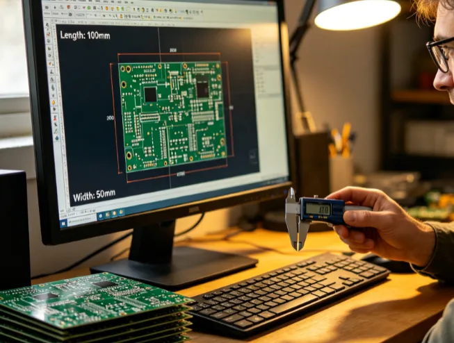
Warpage becomes more noticeable on larger or thinner boards, especially after soldering. Maintaining balanced copper distribution on both sides of the board helps counteract this tendency. Edge clearance and mounting hole placement also require extra attention on bigger designs to prevent cracking during assembly or use. When a project truly needs extended dimensions, discuss panelization options with the fabricator early so that the design remains manufacturable. These steps reduce the chance of boards arriving unusable or requiring costly rework.
Conclusion
Understanding maximum PCB size involves more than picking the largest number available. It requires attention to material behavior, manufacturing equipment limits, and recognized quality standards. Hobbyists who plan dimensions carefully enjoy higher success rates, lower costs, and boards that perform reliably in their projects. Applying these principles consistently turns size from a potential obstacle into a manageable design choice.
FAQs
Q1: What are typical PCB size limits for hobbyist projects?
A1: Hobbyists usually work within dimensions that fit standard manufacturing panels, allowing efficient production of multiple boards at once. Staying inside common panel boundaries helps control cost and improves the likelihood of first-time success. Larger boards remain possible but require extra attention to warpage and handling.
Q2: How do standard PCB sizes affect DIY ordering?
A2: Standard PCB sizes align with the panel formats most fabricators use, which often results in better pricing and faster turnaround. Choosing dimensions that tile efficiently onto a panel reduces waste and simplifies the ordering process. Deviating significantly from these norms may increase cost or require special handling.
Q3: What influences the maximum size of a PCB panel?
A3: Panel size is limited by equipment working areas, material stability, and the need to maintain flatness throughout processing. Larger panels can accommodate bigger individual boards but also raise the risk of dimensional changes during heating and cooling cycles. Following recognized industry specifications helps keep these effects within acceptable ranges.
Q4: Can I order a custom PCB size beyond common dimensions?
A4: Many fabricators accept custom sizes, yet boards that exceed typical panel limits often incur higher costs and longer lead times. It is advisable to confirm the fabricator’s maximum capabilities and any additional requirements before finalizing the design. Starting with a size that respects standard panel constraints usually yields the most predictable results.
References
[IPC-6012E: Qualification and Performance Specification for Rigid Printed Boards]
[IPC-A-600K: Acceptability of Printed Boards]





