In the fast-paced world of electronics manufacturing, ensuring the highest quality for printed circuit boards (PCBs) is critical. One of the most effective ways to achieve this is through Automated Optical Inspection (AOI). But what exactly is AOI, and how does it help maximize PCB quality? In this blog, we’ll explore the benefits and challenges of using AOI in PCB production, providing you with actionable insights to improve your manufacturing process. Whether you’re an engineer or a manufacturer, you’ll find practical information on how this technology can elevate your products while addressing potential hurdles.
What Is Automated Optical Inspection (AOI) in PCB Manufacturing?
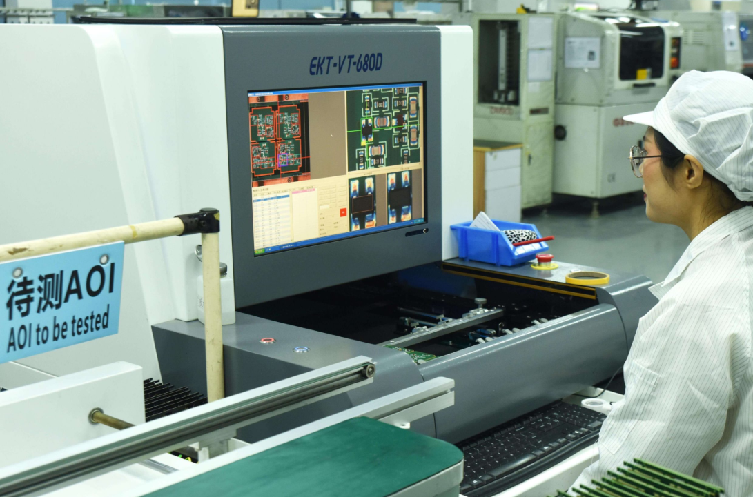
Automated Optical Inspection, or AOI, is a technology used to visually inspect PCBs for defects during the manufacturing process. Using high-resolution cameras and advanced software, AOI systems scan the surface of a PCB to detect issues like missing components, misalignments, solder defects, and other imperfections. Unlike manual inspection, which can be slow and prone to human error, AOI automates the process, ensuring consistency and speed.
In modern PCB assembly lines, where boards are becoming increasingly complex with smaller components and tighter tolerances, AOI plays a vital role. It can inspect thousands of points on a board in seconds, often achieving defect detection rates above 95%, depending on the system and setup. This makes it an indispensable tool for maintaining high-quality standards in large-scale production.
Why PCB Quality Matters More Than Ever
PCBs are the backbone of nearly every electronic device, from smartphones to industrial machinery. A single defect—whether it’s a poor solder joint or a misaligned component—can lead to device failure, costly recalls, or even safety hazards. For industries like automotive or medical, where reliability is non-negotiable, maintaining top-tier PCB quality is essential.
With the rise of miniaturized components (some as small as 0.4mm x 0.2mm) and high-density interconnects, the margin for error has shrunk. Traditional inspection methods struggle to keep up with these demands, often missing subtle defects that can cause significant issues down the line. This is where AOI steps in, offering a reliable solution to catch errors early and ensure that every board meets strict quality standards.
Key Benefits of Automated Optical Inspection (AOI) for PCB Quality
AOI systems bring a range of advantages to PCB manufacturing. Below, we’ll dive into the most significant benefits that help maximize quality and efficiency.
1. Enhanced Accuracy and Defect Detection
AOI systems use high-resolution cameras and sophisticated algorithms to detect defects with precision. They can identify issues like solder bridges, insufficient solder, component misalignment, and even surface scratches that might be invisible to the human eye. Studies show that AOI can achieve defect detection rates of up to 98% for certain types of errors, far surpassing manual inspection capabilities.
For example, in a high-volume production run of 10,000 boards, even a 1% defect rate means 100 faulty units. AOI reduces this risk by catching errors early, often before the board moves to the next assembly stage, saving time and resources.
2. Increased Speed and Efficiency
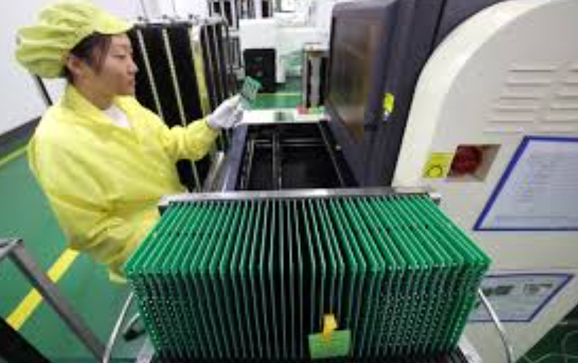
Manual inspection can take several minutes per board, especially for complex designs with hundreds of components. In contrast, AOI systems can inspect a board in under 10 seconds, even for intricate layouts. This speed allows manufacturers to maintain high throughput without sacrificing quality, making it ideal for large-scale production environments.
3. Cost Savings in the Long Run
While the initial investment in AOI equipment can be significant, the long-term cost savings are substantial. By detecting defects early in the production process, AOI prevents faulty boards from reaching later stages or, worse, the end customer. Reworking a defective board after assembly can cost 10 times more than fixing it during production, and recalls can damage a company’s reputation and bottom line.
AOI minimizes these risks, reducing scrap rates and rework costs. For instance, catching a misaligned component during the soldering stage avoids the need for expensive repairs after full assembly.
4. Consistency Across Production Runs
Human inspectors can tire over time, leading to inconsistent results, especially during long shifts. AOI systems, on the other hand, deliver the same level of precision for every board, whether it’s the first or the thousandth in a batch. This consistency ensures that quality standards remain high, even during high-volume production.
5. Data Collection for Process Improvement
Modern AOI systems don’t just detect defects—they also collect data on error types, frequencies, and locations. This information can be used to identify recurring issues in the manufacturing process, such as a specific soldering machine causing defects or a batch of components with alignment problems. By addressing these root causes, manufacturers can continuously improve their processes and prevent future errors.
Challenges of Implementing Automated Optical Inspection (AOI)
While AOI offers numerous benefits, it’s not without its challenges. Understanding these hurdles is crucial for manufacturers looking to integrate this technology effectively. Let’s explore the key obstacles and how they can impact PCB production.
1. High Initial Investment Costs
AOI systems are not cheap. Depending on the complexity and capabilities, a single machine can cost anywhere from $50,000 to over $200,000. For small or medium-sized manufacturers, this upfront cost can be a significant barrier. Additionally, there are expenses related to training staff and maintaining the equipment, which can add to the financial burden.
However, it’s worth noting that the return on investment often justifies the cost, especially for high-volume production where defect reduction directly translates to savings.
2. Complexity in Setup and Programming
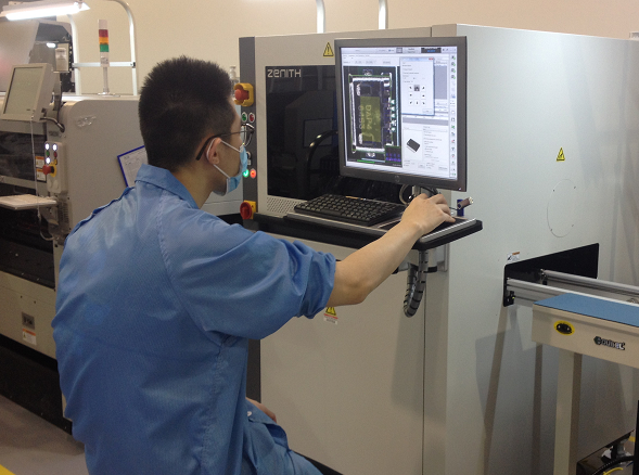
AOI systems require careful setup and programming to function effectively. Each PCB design needs a specific inspection program tailored to its layout and components. Creating these programs can be time-consuming, especially for complex boards with thousands of inspection points. If not programmed correctly, the system might miss defects or flag false positives, reducing its reliability.
For instance, a poorly calibrated AOI system might misinterpret a shiny solder joint as a defect, leading to unnecessary rework and delays. Overcoming this challenge requires skilled technicians and regular system updates.
3. Limitations in Detecting Certain Defects
While AOI excels at identifying surface-level defects, it struggles with issues beneath the surface, such as internal solder joint problems or hidden component failures. For these defects, additional inspection methods like X-ray testing may be necessary. This limitation means that AOI is often used as part of a broader quality control strategy rather than a standalone solution.
For example, a solder joint might look perfect under optical inspection but have a weak internal connection that only an X-ray system can detect. Manufacturers must balance AOI with other testing methods to ensure comprehensive quality control.
4. False Positives and Over-Detection
AOI systems can sometimes be overly sensitive, flagging non-issues as defects. These false positives can slow down production as operators must manually verify each flagged error. In some cases, up to 30% of flagged defects might be false positives, depending on the system’s calibration and the complexity of the board design. This over-detection can lead to inefficiencies and frustration on the production line.
To mitigate this, regular calibration and fine-tuning of the AOI system are essential, along with operator training to quickly distinguish between real and false defects.
5. Adapting to Evolving PCB Designs
As PCB designs evolve with smaller components and more complex layouts, AOI systems must keep up. Older machines may struggle to inspect ultra-fine pitch components (below 0.5mm) or high-density boards, requiring upgrades or replacements. Staying ahead of these technological demands can be challenging, especially for manufacturers with limited budgets.
How to Overcome AOI Challenges and Maximize PCB Quality
Despite the challenges, there are practical steps manufacturers can take to get the most out of AOI systems and ensure top-notch PCB quality. Here are some strategies to consider.
1. Invest in Training and Support
Proper training for operators and technicians is critical to using AOI effectively. Well-trained staff can program the system accurately, interpret results, and minimize false positives. Additionally, partnering with equipment providers for ongoing support and maintenance ensures the system remains reliable over time.
2. Combine AOI with Other Inspection Methods
To address AOI’s limitations, integrate it with complementary technologies like X-ray inspection for internal defects or functional testing for performance issues. This multi-layered approach ensures that all potential problems are caught before the board leaves the production line.
3. Regularly Update and Calibrate Equipment
Keep AOI systems up to date with the latest software and hardware upgrades to handle new PCB designs and component sizes. Routine calibration prevents over-detection and ensures consistent accuracy, reducing downtime caused by false positives.
4. Start Small and Scale Up
For smaller manufacturers concerned about costs, consider starting with a basic AOI system for critical production stages and scaling up as budget allows. This gradual approach minimizes financial strain while still improving quality control.
The Future of AOI in PCB Manufacturing
As technology advances, AOI systems are becoming smarter and more capable. Innovations like 3D AOI, which provides depth perception for more accurate inspections, are gaining traction. These systems can measure component heights and detect issues like lifted leads, offering a significant improvement over traditional 2D AOI.
Additionally, the integration of artificial intelligence (AI) and machine learning is enhancing AOI’s ability to adapt to new designs and reduce false positives. AI-powered systems can learn from past inspections, improving their accuracy over time and identifying subtle defect patterns that older systems might miss.
With these advancements, AOI is poised to remain a cornerstone of PCB quality control, helping manufacturers keep pace with the demands of smaller, more complex electronics.
Conclusion: Striking a Balance with AOI for Optimal PCB Quality
Maximizing PCB quality is a top priority for any electronics manufacturer, and Automated Optical Inspection offers a powerful solution to achieve this goal. With benefits like enhanced accuracy, faster inspections, and long-term cost savings, AOI is transforming the way PCBs are produced. However, challenges such as high costs, setup complexity, and limitations in defect detection require careful planning and strategic implementation.
By understanding both the strengths and weaknesses of AOI, manufacturers can make informed decisions to integrate this technology effectively. Whether it’s through staff training, equipment updates, or combining AOI with other inspection methods, the path to superior PCB quality is within reach. Embracing AOI not only ensures reliable products but also positions manufacturers for success in an increasingly competitive industry.
 ALLPCB


