 ALLPCB


When it comes to military applications, the reliability and durability of electronic components are non-negotiable. One critical element in printed circuit boards (PCBs) used in such high-stakes environments is the gold finger, also known as edge connectors. But what is the ideal PCB gold finger thickness for military applications? In short, gold finger plating thickness typically ranges from 30 to 50 microinches (μ”) of hard gold over a nickel underlayer for military use, balancing durability, conductivity, and insertion lifetime under extreme conditions. This blog post dives deep into the specifics of gold finger thickness, plating processes, and how they impact performance and longevity in military settings.
What Are PCB Gold Fingers and Why Are They Important in Military Applications?
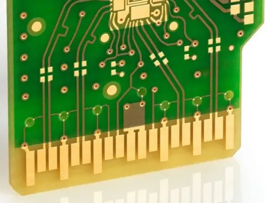
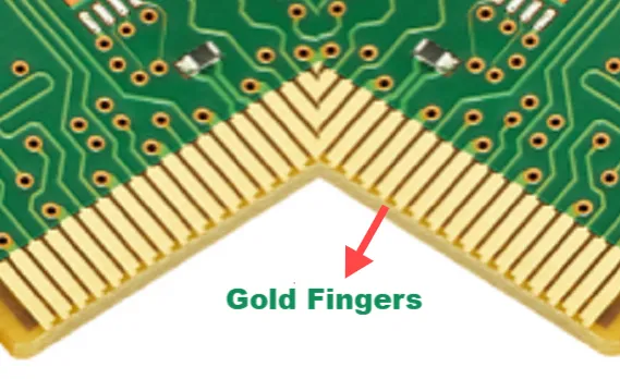
PCB gold fingers are the gold-plated connectors located along the edges of a circuit board. They serve as the interface between the PCB and other components, such as sockets or other boards, facilitating reliable electrical connections. In military applications, where equipment often operates in harsh environments—think extreme temperatures, humidity, vibration, and even exposure to corrosive elements—gold fingers are essential due to their superior conductivity and resistance to corrosion.
Gold, despite being a soft metal, is chosen for its ability to maintain a stable connection over time, unlike other metals that may tarnish or oxidize. For military systems like communication devices, radar systems, and weapon control units, a failed connection could mean mission failure or worse. Therefore, the design and specifications of gold fingers, particularly their thickness, play a pivotal role in ensuring operational success.
The Role of Gold Finger Plating Thickness in Military PCBs
The thickness of the gold plating on PCB fingers is a critical factor that directly affects both performance and durability. In military applications, the plating must withstand repeated insertions and removals, resist wear, and maintain conductivity under stress. Let’s break down why thickness matters and the typical standards used.
Standard Gold Finger Thickness for Military Use
For most military applications, the gold plating thickness on PCB fingers ranges between 30 and 50 microinches (μ”). This range is often paired with a nickel underlayer of 100 to 200 microinches to provide additional strength and prevent diffusion between the gold and the base copper material. The gold itself is typically a "hard gold" alloy, mixed with elements like cobalt or nickel to enhance wear resistance, as pure gold is too soft for repeated use.
This thickness range is chosen based on military standards, such as MIL-DTL-45204, which specifies gold plating requirements for high-reliability applications. A thickness below 30 μ” may lead to premature wear, exposing the underlying nickel or copper and risking corrosion or signal loss. On the other hand, exceeding 50 μ” can increase costs without significant performance gains and may affect insertion forces in high-density connectors.
Balancing Cost and Performance
While thicker gold plating might seem like the obvious choice for durability, it comes with higher manufacturing costs. Military projects often operate under strict budgets, so engineers must balance the need for reliability with economic constraints. A plating thickness of 30 μ” is often sufficient for applications with moderate insertion cycles (e.g., 200-500 cycles), while 50 μ” is preferred for systems requiring over 1,000 insertion cycles.
Insertion Lifetime: How Gold Finger Thickness Affects Longevity
Insertion lifetime refers to the number of times a PCB can be plugged into and removed from a connector before the gold fingers show significant wear or loss of conductivity. In military applications, where equipment may be frequently maintained or upgraded, insertion lifetime is a key performance metric.
Factors Impacting Insertion Lifetime
The thickness of the gold plating directly influences how many insertion cycles a PCB can endure. For instance, a gold layer of 30 μ” can typically withstand around 200 to 500 insertion cycles before the plating begins to wear down, exposing the nickel underlayer. At 50 μ”, this can extend to 1,000 cycles or more, depending on the connector design and environmental conditions.
Other factors also play a role, such as:
- Connector Design: High-density connectors with tighter tolerances can increase wear on gold fingers, reducing insertion lifetime.
- Environmental Conditions: Exposure to dust, moisture, or corrosive gases can accelerate wear, even with thicker plating.
- Insertion Force: Excessive force during insertion or removal can damage the plating, shortening its lifespan.
Military Standards for Insertion Lifetime
Military specifications often demand a minimum insertion lifetime to ensure reliability. For example, systems adhering to MIL-STD-810 (a standard for environmental testing) may require gold fingers to endure at least 500 insertion cycles under simulated field conditions, including temperature extremes from -55°C to 125°C and vibration levels up to 20G. A plating thickness of at least 30 μ” is typically necessary to meet these rigorous demands, with higher thicknesses used for more critical applications.
Gold Plating Process for Military-Grade PCBs
The process of applying gold plating to PCB fingers is as important as the thickness itself. Military applications require a precise, high-quality plating process to ensure consistent performance. Here’s an overview of how it’s done and why it matters.
Electroplating Hard Gold
The most common method for gold finger plating in military PCBs is electroplating hard gold over a nickel underlayer. The process involves:
- Nickel Underplating: A layer of nickel, typically 100-200 μ” thick, is applied to the copper base of the PCB edge. This acts as a barrier to prevent diffusion and adds mechanical strength.
- Hard Gold Plating: A thin layer of hard gold (30-50 μ”) is then electroplated onto the nickel. Hard gold is an alloy, often mixed with cobalt, to improve wear resistance compared to soft gold.
This two-layer approach ensures that the gold fingers can handle the mechanical stress of repeated insertions while maintaining excellent electrical conductivity (approximately 4.1 μΩ·cm resistivity for gold).
Beveling for Enhanced Performance
In military PCBs, gold fingers are often beveled at a 30-45-degree angle at the edge. This beveling reduces insertion force and minimizes wear on the plating during connection, extending the insertion lifetime. It’s a small but critical detail that can make a significant difference in high-reliability applications.
Challenges and Considerations for Military PCB Gold Fingers
Designing and manufacturing gold fingers for military use comes with unique challenges. Engineers must consider several factors to ensure the final product meets the stringent requirements of defense applications.
Environmental Durability
Military equipment often operates in extreme conditions, from desert heat to arctic cold. Gold fingers must resist corrosion and maintain conductivity even after prolonged exposure to salt spray (tested per MIL-STD-810), high humidity, or chemical contaminants. A thicker gold layer (closer to 50 μ”) is often necessary for such environments to prevent wear-through.
Signal Integrity
In high-frequency military systems like radar or communication devices, signal integrity is paramount. Gold fingers must provide low contact resistance (typically below 10 milliohms) to prevent signal loss. The plating thickness and quality directly impact this, as insufficient gold can lead to increased resistance over time due to wear.
Cost vs. Reliability
As mentioned earlier, thicker gold plating increases manufacturing costs. For military projects with tight budgets, engineers often opt for the minimum viable thickness (around 30 μ”) that still meets reliability standards. However, for mission-critical systems, the extra cost of 50 μ” plating is often justified by the added durability.
Best Practices for Designing Gold Fingers in Military PCBs
To maximize the performance and lifespan of gold fingers in military applications, consider the following best practices during design and manufacturing:
- Adhere to Military Standards: Follow guidelines like MIL-DTL-45204 for gold plating and MIL-STD-810 for environmental testing to ensure compliance and reliability.
- Choose the Right Thickness: Select a plating thickness (30-50 μ”) based on the expected insertion cycles and environmental conditions.
- Use Hard Gold: Opt for hard gold alloys over soft gold to improve wear resistance for repeated insertions.
- Incorporate Beveling: Design beveled edges to reduce insertion force and minimize plating wear.
- Test Rigorously: Conduct thorough testing for insertion lifetime, contact resistance, and environmental durability to validate performance before deployment.
Conclusion: Ensuring Reliability with the Right Gold Finger Thickness
In military applications, where failure is not an option, the thickness of PCB gold fingers is a critical design consideration. A plating thickness of 30 to 50 microinches of hard gold over a nickel underlayer provides the necessary balance of conductivity, durability, and insertion lifetime to meet the demands of harsh environments and rigorous use. By understanding the interplay between plating thickness, environmental factors, and insertion cycles, engineers can design PCBs that deliver reliable performance in the field.
Whether it’s for communication systems, weapon controls, or radar equipment, the right gold finger specifications ensure that military electronics operate without interruption. By adhering to established standards and best practices, manufacturers can produce high-quality PCBs tailored to the unique challenges of defense applications. At ALLPCB, we’re committed to supporting engineers with the expertise and manufacturing capabilities needed to bring these critical designs to life.


