ALLPCB


If you're looking to understand how selective PCB gold fingers are manufactured using blue glue, you're in the right place. This process involves applying a protective blue glue mask to ensure precise hard gold plating on gold finger pads while protecting other areas of the PCB surface. In this detailed guide, we'll walk you through the entire process, from the role of blue glue to the benefits of electroless nickel immersion gold (ENIG) and hard gold plating. Whether you're an engineer or a procurement specialist working with PCB manufacturers, this blog will provide actionable insights into creating durable and reliable gold finger pads for your projects.
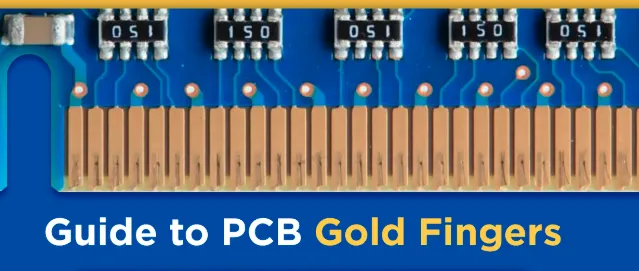
What Are PCB Gold Fingers and Why Are They Important?
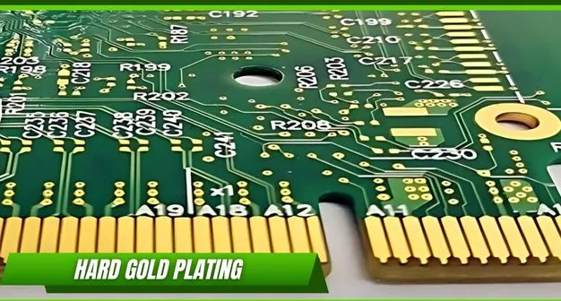
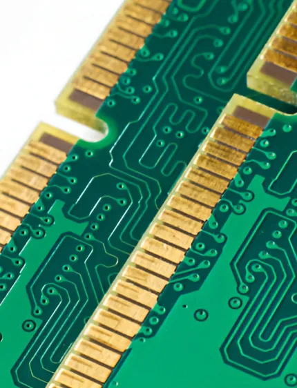
PCB gold fingers, often called edge connectors, are the gold-plated pads located along the edges of a printed circuit board (PCB). These metallic contacts are designed to connect the PCB to other components or systems, such as in computer memory modules or industrial control systems. The gold plating on these pads ensures excellent conductivity, corrosion resistance, and durability, even after repeated insertions and removals.
The importance of gold fingers lies in their ability to maintain reliable connections over time. Without proper plating, the pads could wear out, leading to signal loss or device failure. For instance, in high-frequency applications, a poorly plated gold finger can result in impedance mismatches, affecting signal speeds that often range from 1 GHz to 5 GHz in modern electronics. This is why manufacturing gold fingers with precision and the right materials is critical for PCB performance.
The Role of Blue Glue in Selective Gold Finger Manufacturing
Blue glue, a type of peelable solder mask, plays a vital role in the selective manufacturing of PCB gold fingers. During the production process, certain areas of the PCB need to be protected from plating or soldering. Blue glue is applied to these areas as a temporary mask, ensuring that only the designated gold finger pads receive the hard gold plating or electroless nickel immersion gold (ENIG) finish.
The glue is typically applied using a screen-printing method, covering parts of the PCB surface that should remain free of gold or nickel. Its vibrant blue color makes it easy to identify during manufacturing, ensuring accuracy. Once the plating process is complete, the blue glue can be peeled off without leaving residue, revealing the protected areas underneath. This selective approach saves costs by limiting the use of expensive gold plating to only the necessary regions, such as the gold finger pads.
Understanding Hard Gold Plating for Gold Fingers
Hard gold plating is a popular choice for PCB gold fingers due to its durability and wear resistance. Unlike soft gold, which is purer and more prone to scratching, hard gold is alloyed with small amounts of cobalt or nickel to increase its hardness. This makes it ideal for edge connectors that experience frequent mating and unmating cycles, such as in server boards or graphics cards.
The thickness of hard gold plating typically ranges from 10 to 50 microinches (0.25 to 1.27 micrometers), depending on the application. For example, a thickness of 30 microinches is often used for gold fingers in consumer electronics to balance cost and performance. This plating is applied over a base layer of nickel, which acts as a barrier to prevent diffusion between the copper substrate and the gold layer, enhancing the lifespan of the gold finger pads.
Hard gold plating ensures that the gold fingers can withstand up to 1,000 mating cycles without significant wear, making it a reliable choice for high-usage applications. However, it is more expensive than other finishes, which is why selective plating with blue glue is often used to target only the necessary areas.
Electroless Nickel Immersion Gold (ENIG) in PCB Manufacturing
Electroless Nickel Immersion Gold, commonly known as ENIG, is another widely used surface finish in PCB manufacturing, often applied alongside or as an alternative to hard gold plating for gold fingers. ENIG involves depositing a layer of nickel through an electroless process, followed by a thin layer of immersion gold, typically 2 to 5 microinches (0.05 to 0.13 micrometers) thick. This finish provides excellent solderability and corrosion resistance for the PCB surface.
While ENIG is not as durable as hard gold plating for high-wear applications, it is often used for gold fingers in less demanding environments. It is also more cost-effective, making it a preferred choice for PCB manufacturers looking to balance performance and budget. Additionally, ENIG offers a flat surface finish, which is beneficial for fine-pitch components on the PCB surface outside the gold finger area.
One challenge with ENIG is the potential for "black pad" defects, where the nickel layer corrodes due to improper processing, leading to poor solder joints. However, with strict quality control during manufacturing, this issue can be minimized, ensuring reliable gold finger pads.
Step-by-Step Process of Manufacturing Selective Gold Fingers Using Blue Glue
Manufacturing selective PCB gold fingers using blue glue involves several precise steps to ensure quality and functionality. Below is a detailed breakdown of the process:
- Design and Preparation: The PCB layout is designed with gold finger pads along the edges. Specifications for plating thickness and materials (hard gold or ENIG) are determined based on the application requirements.
- Application of Blue Glue: A peelable blue glue mask is applied to areas of the PCB surface that should not receive gold plating. This is done using screen printing to ensure accuracy, covering all non-gold finger regions.
- Nickel Underplating: A layer of nickel, typically 100 to 200 microinches (2.54 to 5.08 micrometers) thick, is deposited on the exposed gold finger pads. This acts as a barrier layer to prevent copper diffusion and enhance adhesion for the gold layer.
- Gold Plating: Depending on the chosen finish, hard gold plating or immersion gold (for ENIG) is applied to the gold finger pads. For hard gold, the thickness is controlled to meet durability needs, often around 30 microinches for standard applications.
- Removal of Blue Glue: After plating, the blue glue mask is peeled off, revealing the protected areas of the PCB surface. This step ensures that only the gold fingers are plated, reducing material costs.
- Inspection and Testing: The gold fingers are inspected for plating thickness, adhesion, and surface quality. Tests may include measuring contact resistance (typically below 10 milliohms) to ensure reliable performance.
This selective process, aided by blue glue, allows PCB manufacturers to produce high-quality gold fingers efficiently while minimizing waste and cost.
Benefits of Using Blue Glue for Selective Gold Plating
Using blue glue in the manufacturing of selective PCB gold fingers offers several advantages, especially for engineers and manufacturers looking to optimize production. Here are some key benefits:
- Cost Efficiency: By masking off unnecessary areas, blue glue ensures that expensive gold plating is applied only to gold finger pads, reducing material costs significantly.
- Precision: The screen-printing application of blue glue allows for precise coverage, ensuring that only the intended areas are plated, which is critical for maintaining PCB design integrity.
- Easy Removal: Blue glue can be peeled off cleanly after plating, leaving no residue on the PCB surface and simplifying the manufacturing process.
- Versatility: This method works well with both hard gold plating and ENIG finishes, making it adaptable to various project requirements.
For example, in a batch production of 10,000 PCBs for industrial controllers, using blue glue could save thousands of dollars in gold material costs by limiting plating to the edge connectors.
Challenges in Manufacturing Gold Fingers and How to Overcome Them
While manufacturing PCB gold fingers using blue glue is effective, there are challenges that manufacturers face. Understanding these issues and their solutions can help ensure a smoother production process.
- Uneven Plating Thickness: Variations in gold or nickel thickness can affect conductivity and durability. Using automated plating equipment with precise control can maintain consistent thicknesses, such as 30 microinches for hard gold.
- Blue Glue Residue: If not properly applied or removed, blue glue can leave residue on the PCB surface, affecting aesthetics or functionality. Thorough cleaning and quality checks after removal can prevent this issue.
- High Costs of Hard Gold: Hard gold plating is expensive, especially for large-scale production. Selective plating with blue glue and opting for ENIG where possible can help manage costs without compromising quality.
By addressing these challenges, PCB manufacturers can deliver reliable gold finger pads that meet the stringent demands of modern electronics.
Choosing the Right PCB Manufacturer for Gold Finger Production
Selecting a reliable PCB manufacturer is crucial for achieving high-quality gold fingers with the desired surface finish. Here are some factors to consider when partnering with a manufacturer for your projects:
- Experience with Selective Plating: Ensure the manufacturer has expertise in using blue glue for selective hard gold plating or ENIG finishes on gold finger pads.
- Quality Control Standards: Look for manufacturers with strict testing protocols, such as measuring plating thickness and contact resistance, to guarantee performance.
- Customization Options: The manufacturer should offer flexibility in gold finger design, including varying lengths, shapes, and plating thicknesses to suit your specific needs.
- Cost-Effective Solutions: A good manufacturer will help optimize costs by using selective plating techniques like blue glue masking without sacrificing quality.
Working with a trusted manufacturer ensures that your PCB gold fingers are built to last, even in demanding applications like telecommunications or automotive systems.
Conclusion: Optimizing PCB Gold Fingers with Blue Glue
Manufacturing selective PCB gold fingers using blue glue is a proven method to achieve precision, durability, and cost efficiency in PCB production. By protecting non-essential areas of the PCB surface with blue glue, manufacturers can focus hard gold plating or electroless nickel immersion gold (ENIG) only on the gold finger pads, ensuring optimal performance where it matters most. This approach not only reduces costs but also maintains the high standards required for reliable edge connectors in modern electronics.
Whether you're designing PCBs for consumer gadgets or industrial equipment, understanding the role of blue glue in selective plating can help you make informed decisions. Partnering with experienced PCB manufacturers who prioritize quality and customization will further ensure that your gold fingers meet the specific demands of your application, from signal integrity to long-term durability.
With the right techniques and expertise, the use of blue glue in manufacturing PCB gold fingers can elevate the quality of your products, making them stand out in a competitive market. If you're ready to start your next project, focus on precision and reliability by leveraging this innovative approach to PCB surface finishing.