 ALLPCB


In the fast-paced world of electronics, high-speed PCB design is crucial for meeting the demands of modern devices. One key technique that stands out for improving performance is PCB back drilling. But what exactly is back drilling, and is it a cost-effective solution for high-speed applications? Simply put, PCB back drilling is a manufacturing process that removes unused portions of via stubs in through-hole vias, enhancing signal integrity by reducing signal reflections and noise. It’s especially valuable in high-speed designs where signal clarity is critical, and while it adds to production costs, the benefits often outweigh the expenses for many projects.
In this comprehensive guide, we’ll dive deep into the world of PCB back drilling, exploring its benefits for high-speed PCB design, how it impacts signal integrity, and whether it’s a cost-effective solution for your needs. Whether you’re an engineer working on cutting-edge technology or a designer looking to optimize performance, this blog will provide actionable insights into using back drilling to tackle via stubs and achieve better results.
What Is PCB Back Drilling?
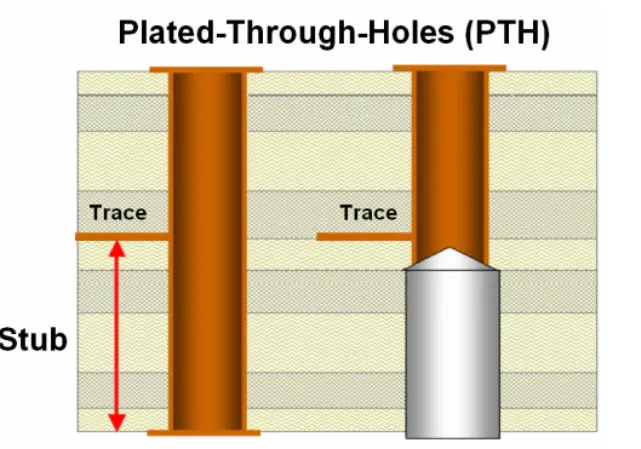
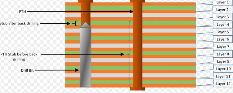
PCB back drilling, also known as controlled depth drilling, is a specialized manufacturing technique used in printed circuit board (PCB) fabrication. It involves drilling into a PCB from the opposite side of a through-hole via to remove the unused portion of the via barrel, known as a via stub. These stubs are leftover conductive sections of a via that aren’t part of the active signal path. In high-speed applications, via stubs can cause signal reflections, distortions, and noise, which degrade performance.
By removing these stubs, back drilling minimizes signal integrity issues, making it a go-to solution for designs operating at high frequencies, such as those in telecommunications, data centers, and advanced computing. The process uses a slightly larger drill bit than the original via hole to ensure the stub is removed without damaging the functional part of the via. This precision is what makes back drilling effective, though it does require advanced equipment and expertise.
Why Back Drilling Matters for High-Speed PCB Design
In high-speed PCB design, maintaining signal integrity is a top priority. As signal speeds increase—often exceeding 10 Gbps in modern applications—small imperfections in the PCB can lead to big problems. Via stubs are one such imperfection. They act like tiny antennas, causing signal reflections that interfere with data transmission. This can result in errors, reduced performance, and even complete system failures in critical applications.
Back drilling addresses this issue directly by eliminating via stubs. For instance, in a multilayer PCB with a signal transitioning between layers, a via stub might resonate at certain frequencies, creating a mismatch in impedance. Without back drilling, this mismatch could cause signal loss or crosstalk. By removing the stub, the signal path is cleaner, and impedance is better controlled, often staying within a target range like 50 ohms for many high-speed designs.
Beyond impedance control, back drilling also reduces electromagnetic interference (EMI) and improves overall reliability. This makes it an essential technique for applications like 5G infrastructure, high-performance computing, and automotive radar systems, where even minor signal degradation can have significant consequences.
Signal Integrity: The Core Benefit of Back Drilling
Signal integrity refers to the quality of an electrical signal as it travels through a PCB. Poor signal integrity leads to data errors, timing issues, and reduced system performance. In high-speed designs, factors like via stubs, crosstalk, and signal loss are major threats to signal integrity. Back drilling specifically targets via stubs, which are a common culprit in signal degradation.
Here’s how via stubs impact signal integrity: when a high-speed signal passes through a via with an unused stub, part of the signal energy travels down the stub and reflects back, interfering with the main signal. This reflection can cause jitter, eye diagram closure, and bit errors. For example, at signal speeds of 25 Gbps, even a short stub of 0.5 mm can create noticeable reflections. Back drilling removes this stub, ensuring the signal travels only along the intended path, thus preserving its integrity.
The result? Cleaner signals, lower bit error rates, and better overall performance. This is especially critical in applications where timing is everything, such as DDR4 memory interfaces or high-speed serial links like PCIe 4.0 and 5.0.
PCB Back Drilling Cost: Is It Worth the Investment?
One of the most common concerns about PCB back drilling is the cost. Back drilling is an additional manufacturing step that requires specialized equipment, skilled operators, and precise process control. Naturally, this increases the overall production cost of the PCB. However, the question isn’t just about the upfront PCB back drilling cost—it’s about whether the investment delivers enough value to justify it.
The cost of back drilling varies depending on factors like board complexity, the number of vias to be drilled, and the layer count. For a typical high-speed design, back drilling can add anywhere from 10% to 30% to the fabrication cost. While this might seem steep, the benefits often outweigh the expense in high-speed applications. For example, without back drilling, you might face costly redesigns or system failures due to poor signal integrity. In contrast, investing in back drilling upfront can save significant time and money by ensuring the design performs as expected from the start.
Moreover, not every project needs back drilling. For lower-speed designs (below 5 Gbps), the impact of via stubs is often negligible, and alternative techniques like proper via placement or shorter stubs through design optimization might suffice. However, for designs pushing 10 Gbps and beyond, back drilling becomes a cost-effective solution compared to the potential risks of signal issues.
Cost-Effective Solutions: Balancing Performance and Budget
While back drilling is a powerful tool for high-speed PCB design, it’s not the only option. Designers looking for cost-effective solutions can combine back drilling with other strategies to balance performance and budget. Here are a few approaches to consider:
- Selective Back Drilling: Instead of back drilling every via, focus only on critical high-speed signal paths. This reduces manufacturing costs while still addressing the most pressing signal integrity concerns.
- Optimized Layer Stackup: Design the PCB stackup to minimize via stub length by routing high-speed signals on outer layers or using fewer layer transitions. This can reduce the need for extensive back drilling.
- Blind and Buried Vias: As an alternative to through-hole vias, blind and buried vias eliminate stubs entirely by not extending through the full board thickness. While these vias can be more expensive to fabricate, they might reduce or eliminate the need for back drilling in some designs.
By combining these techniques, you can achieve a cost-effective solution that meets the performance requirements of your high-speed application without breaking the bank. The key is to analyze the specific needs of your design and prioritize back drilling where it will have the most impact.
How Back Drilling Fits Into High-Speed PCB Design Workflow
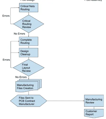
Integrating back drilling into your high-speed PCB design process requires careful planning. It’s not just a manufacturing step—it’s a design consideration that affects layout, simulation, and testing. Here’s how to incorporate back drilling effectively:
1. Identify Critical Vias: During the design phase, use simulation tools to identify vias that carry high-speed signals and are likely to have problematic stubs. Focus back drilling efforts on these areas.
2. Collaborate with Fabricators: Work closely with your PCB manufacturer to ensure they have the capability to perform back drilling with the required precision. Provide clear documentation on which vias need drilling and to what depth.
3. Simulate and Test: After fabrication, use signal integrity testing to verify that back drilling has resolved the expected issues. Tools like time-domain reflectometry (TDR) can help measure impedance and confirm the absence of reflections.
By embedding back drilling into your workflow, you can ensure that it’s applied strategically, maximizing its benefits while keeping costs in check.
Challenges and Limitations of Back Drilling
While back drilling offers significant advantages, it’s not without challenges. Understanding these limitations can help you make informed decisions about when and how to use it.
First, back drilling requires high precision. If the drill depth isn’t controlled accurately, it can damage the functional part of the via or leave residual stubs, negating the benefits. This precision comes at a cost, both in terms of equipment and time.
Second, back drilling isn’t suitable for all designs. In very dense boards with closely spaced vias, there’s a risk of damaging adjacent structures during drilling. Additionally, back drilling can weaken the board’s mechanical structure if too many vias are processed, especially in thinner boards.
Finally, back drilling adds complexity to the manufacturing process, which can lead to longer lead times. For projects with tight deadlines, this delay might be a significant drawback.
When to Choose Back Drilling for Your Project
Deciding whether to use back drilling comes down to the specific requirements of your project. Here are some scenarios where it’s likely the right choice:
- High-Speed Signals: If your design involves signals above 10 Gbps, back drilling is often necessary to maintain signal integrity.
- Multilayer Boards: In boards with many layers, via stubs are more common and problematic, making back drilling a valuable solution.
- Critical Applications: For mission-critical systems like aerospace or medical devices, the cost of back drilling is justified by the need for flawless performance.
On the other hand, for low-speed or less complex designs, the added cost and time of back drilling might not be worth it. Always weigh the performance benefits against the PCB back drilling cost and project constraints.
Future Trends in Back Drilling and High-Speed Design
As technology continues to advance, the role of back drilling in high-speed PCB design is likely to evolve. With signal speeds pushing toward 100 Gbps and beyond, the demand for techniques that preserve signal integrity will only grow. Innovations in manufacturing equipment are making back drilling more precise and affordable, potentially reducing costs in the future.
Additionally, new design methodologies, such as advanced simulation tools and automated via optimization, may complement back drilling, allowing designers to minimize stubs even before fabrication. These trends suggest that while back drilling will remain a key technique, it will be part of a broader toolkit for achieving cost-effective solutions in high-speed applications.
Conclusion: Back Drilling as a Strategic Choice for High-Speed PCBs
PCB back drilling stands out as a powerful and often cost-effective solution for high-speed applications. By eliminating via stubs, it directly addresses signal integrity challenges, ensuring cleaner signals and better performance in demanding environments. While the PCB back drilling cost is a consideration, the benefits—reduced signal reflections, lower error rates, and improved reliability—often make it a worthwhile investment for designs operating at 10 Gbps and above.
For engineers and designers, the key to success lies in understanding when and how to apply back drilling. By combining it with other cost-effective solutions like selective drilling and optimized stackups, you can strike the right balance between performance and budget. As high-speed PCB design continues to push boundaries, techniques like back drilling will play a critical role in meeting the challenges of tomorrow’s technology.
At ALLPCB, we’re committed to supporting your high-speed design needs with advanced manufacturing capabilities and expert guidance. Whether you’re tackling via stubs or optimizing signal integrity, our team is here to help you achieve the best results for your project.


