 ALLPCB


In the world of printed circuit board (PCB) design, achieving optimal performance while minimizing issues like electromagnetic interference (EMI) is a top priority for engineers. Two critical aspects of this process are PCB impedance control and EMI reduction. But how do these concepts work together to ensure a reliable and compliant design? In short, impedance control ensures signal integrity by managing electrical characteristics of traces, while EMI reduction techniques like grounding and shielding protect against interference. This blog dives deep into both topics, offering practical strategies for EMC compliance, addressing impedance discontinuity, and optimizing your PCB layout with effective PCB grounding and shielding methods.
Whether you're designing for high-speed applications or sensitive electronics, this comprehensive guide will walk you through the essentials of impedance control and EMI reduction. Let’s explore how these principles can elevate your PCB designs to meet modern standards.
What is PCB Impedance Control and Why Does It Matter?
Impedance control in PCB design refers to the management of the electrical impedance of traces on a board to ensure consistent signal transmission. Impedance, measured in ohms, is the resistance to the flow of alternating current (AC) in a circuit. When designing high-speed circuits, maintaining a specific impedance—often 50 ohms or 75 ohms—is crucial to prevent signal reflections and ensure data integrity.
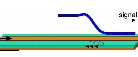
Without proper impedance control, signals can degrade due to reflections caused by impedance discontinuity. This happens when there’s a mismatch between the impedance of a trace and the connected components or transmission lines. For example, a high-speed signal traveling at 3 GHz could experience significant loss if the trace impedance varies by even 10%. Such issues can lead to data errors, slower performance, and even system failures in critical applications like telecommunications or medical devices.
Impedance control is achieved by carefully designing the trace width, spacing, and dielectric materials of the PCB. Tools like impedance calculators and simulation software help engineers predict and adjust these parameters during the design phase. By maintaining consistent impedance, you also reduce the risk of EMI, as erratic signals are less likely to radiate unwanted electromagnetic energy.
Understanding EMI and Its Impact on PCB Performance
Electromagnetic interference (EMI) is the unwanted noise or disturbance in an electronic system caused by external or internal electromagnetic fields. EMI can disrupt signal integrity, degrade performance, and even cause complete system failures. As devices become smaller and operate at higher frequencies (often exceeding 1 GHz), the risk of EMI increases significantly.
EMI can be radiated (traveling through the air) or conducted (traveling through power lines or traces). Both types pose challenges to achieving EMC compliance, which is the ability of a device to operate without interfering with other systems or being affected by external interference. Regulatory bodies worldwide, such as the FCC in the United States or the EU’s CE marking requirements, enforce strict EMI limits to ensure devices meet these standards.
Effective EMI reduction starts at the PCB design stage. By implementing strategies like proper grounding, shielding, and layout optimization, you can minimize EMI risks and ensure your design passes compliance tests.
Key Techniques for EMI Reduction in PCB Design
Let’s break down some of the most effective methods for reducing EMI in your PCB designs. These techniques focus on layout, grounding, and shielding to create a robust defense against interference.
1. Optimize PCB Grounding for EMI Reduction
PCB grounding is one of the most fundamental steps in controlling EMI. A well-designed ground plane acts as a reference point for signals and provides a low-impedance path for return currents, reducing the likelihood of noise coupling.
To optimize grounding, use a solid ground plane rather than a split or fragmented one, especially in high-speed designs. A continuous ground plane beneath signal traces can reduce loop areas, which are prime sources of radiated EMI. For instance, a loop area of just 1 square centimeter can act as an antenna, radiating noise at frequencies above 100 MHz. Placing ground vias near signal vias also helps maintain a short return path, further minimizing interference.
Additionally, separate analog and digital grounds if your design includes mixed-signal components. This prevents noisy digital signals from interfering with sensitive analog circuits. Connect these grounds at a single point to avoid ground loops, which can amplify EMI.
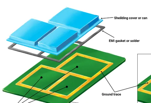
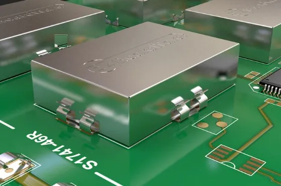
2. Implement Effective Shielding Techniques
Shielding is another powerful tool for EMI reduction. It involves enclosing sensitive components or entire sections of a PCB in conductive materials to block external electromagnetic fields or contain internal emissions.
Common shielding methods include using metal enclosures or cans over critical components like RF modules. On the PCB level, you can add copper pour areas connected to ground around sensitive traces to act as a Faraday cage. For high-frequency designs, ensure the shield is properly grounded to avoid creating unintended antennas that could worsen EMI.
Shielding is particularly important in densely packed designs where components are close together, increasing the risk of crosstalk. For example, in a 5G communication board operating at 3.5 GHz, shielding can reduce crosstalk by up to 20 dB, significantly improving performance.
3. Minimize Impedance Discontinuity in High-Speed Designs
As mentioned earlier, impedance discontinuity can lead to signal reflections, which not only degrade performance but also contribute to EMI. To minimize discontinuities, ensure that traces maintain consistent width and spacing, especially when transitioning between layers through vias.
Use controlled impedance routing for high-speed signals, matching the trace impedance to the source and load. For example, a USB 3.0 signal requires a differential impedance of 90 ohms ±10% to avoid reflections. Avoid sharp bends in traces—opt for 45-degree angles or curves to maintain signal integrity. Additionally, place decoupling capacitors close to power pins to stabilize voltage and reduce noise that could radiate as EMI.
4. Optimize Component Placement and Trace Routing
Component placement and trace routing play a significant role in EMI reduction. Place noisy components, such as switching regulators, away from sensitive circuits like analog sensors. Keep high-speed traces short and direct to minimize their ability to act as antennas. For instance, a trace longer than 1/10th of the wavelength of the signal frequency can radiate significant EMI.
Route power and ground traces first to establish a stable reference, then route high-speed signals with minimal crossings over splits in the ground plane. Use differential pairs for high-speed signals to cancel out common-mode noise, a common source of EMI.
Combining Impedance Control with EMI Reduction for EMC Compliance
Achieving EMC compliance requires a holistic approach that integrates impedance control and EMI reduction strategies. EMC standards test both emissions (how much interference your device produces) and immunity (how well it resists external interference). Failing these tests can delay product launches and incur costly redesigns.
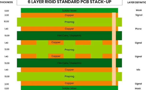
Start by designing for controlled impedance to ensure clean signal transmission, which inherently reduces radiated EMI. Then, layer in grounding and shielding techniques to further suppress interference. For example, in a multilayer PCB for an industrial control system, a 4-layer stackup with dedicated ground and power planes can reduce EMI by up to 30% compared to a 2-layer design.
Simulate your design using electromagnetic compatibility software to identify potential EMI hotspots before fabrication. Tools like these can predict how a 2.4 GHz Wi-Fi signal might interfere with nearby traces and suggest layout adjustments. Finally, test prototypes in an EMC lab to confirm compliance with standards like CISPR or MIL-STD-461, depending on your application.
Practical Tips for Implementing Impedance Control and EMI Reduction
Here are some actionable tips to help you apply these concepts in your next PCB design:
- Use PCB design software with built-in impedance calculators to set trace dimensions accurately.
- Choose dielectric materials with consistent properties (e.g., FR-4 with a dielectric constant of 4.2-4.5) to maintain impedance stability.
- Add stitching vias around the board edges to connect ground planes across layers, reducing EMI.
- Place ferrite beads or filters on power lines to suppress high-frequency conducted noise.
- Keep clock signals away from board edges to prevent them from radiating EMI.
Challenges and Solutions in High-Speed PCB Design
High-speed PCB designs present unique challenges for both impedance control and EMI reduction. As signal frequencies climb into the gigahertz range, even small variations in trace length or material properties can cause issues. For instance, a 5% mismatch in impedance on a 10 GHz signal can lead to a 20% signal loss due to reflections.
To address this, consider using advanced materials with lower dielectric losses for high-frequency applications. Additionally, adopt back-drilling techniques to remove unused via stubs, which can cause impedance discontinuities. For EMI, integrate on-board filtering using capacitors and inductors to dampen noise at the source.
Conclusion: Building Better PCBs with Impedance Control and EMI Reduction
Mastering PCB impedance control and EMI reduction is essential for designing reliable, high-performance electronics. By focusing on controlled impedance, you ensure signal integrity and minimize reflections that contribute to EMI. At the same time, techniques like PCB grounding, shielding, and layout optimization help mitigate interference, paving the way for EMC compliance.
Whether you’re working on consumer gadgets, industrial systems, or cutting-edge communication devices, these strategies can make a significant difference in your design’s success. Start by integrating these practices into your workflow, from initial simulations to final testing, and watch as your PCBs achieve better performance with fewer interference issues. With a comprehensive approach, you can tackle impedance discontinuity and EMI challenges head-on, delivering products that meet the highest standards of quality and reliability.


