 ALLPCB


What Is Liquid Photoimageable Solder Mask and Why It Matters
Liquid photoimageable solder mask consists of a photosensitive polymer applied in liquid form to the PCB surface. Once cured, it forms a durable insulating coating that prevents solder bridging and protects against oxidation, moisture, and mechanical damage. The material stands out for its ability to conform to surface topography, including traces and vias of varying heights. Industry relevance stems from the demand for higher interconnect densities in consumer electronics, automotive systems, and telecommunications equipment. Designers specify this solder mask type when trace widths and spacings fall below thresholds achievable with alternative methods. Proper application supports electrical isolation requirements and thermal performance during reflow operations.
Technical Principles and Mechanisms
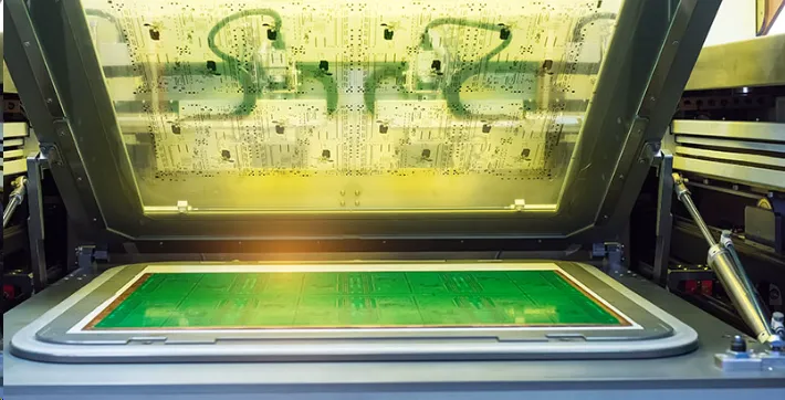
The core mechanism relies on photopolymerization. Ultraviolet light exposure initiates crosslinking in designated regions of the liquid coating. Unexposed areas remain soluble and are removed during the development stage. This selective curing produces sharp edges and accurate registration to the underlying copper pattern. Application methods such as spray coating or curtain coating distribute the material evenly across the board. A subsequent drying step removes solvents and prepares the surface for exposure. Development typically employs an alkaline solution that dissolves the unpolymerized mask without affecting cured sections. Final thermal curing completes the crosslinking and enhances mechanical properties. Thickness control remains essential because it influences dielectric strength and coverage over copper features. Variations in exposure energy and development parameters directly affect resolution and adhesion. These steps follow structured sequences to maintain consistency across production batches.
Applying LPI Solder Mask: Practical Process Steps and Best Practices
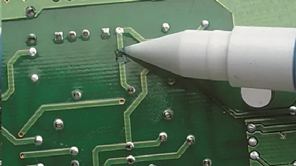
Surface preparation begins with thorough cleaning to remove contaminants that could impair adhesion. Boards undergo chemical or mechanical treatments to ensure a uniform base for coating. Application follows using controlled equipment to achieve target thickness, often in the range that meets performance criteria. Multiple passes or adjustments in viscosity help accommodate different board designs. After coating, a pre-bake or tack-dry stage stabilizes the film before imaging. Precise alignment of the exposure tool with the circuit pattern ensures accurate solder mask openings. Development removes excess material from pads and holes while preserving the protective coating elsewhere. Post-development inspection verifies registration and coverage before the final cure cycle. Engineers monitor parameters such as exposure dose, development time, and cure temperature to optimize results. Compatibility between the solder mask chemistry and the laminate material prevents issues like delamination during subsequent thermal excursions. Documentation of process variables supports traceability and repeatability in manufacturing environments.
LPI Solder Mask Advantages in Engineering Applications
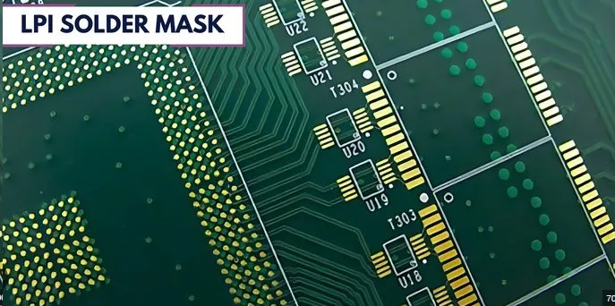
The liquid photoimageable solder mask process delivers superior resolution compared with certain dry film alternatives, enabling finer dams between closely spaced pads. This capability proves valuable for fine-pitch components and high-density interconnect designs. Conformal coverage reduces the risk of exposed copper on irregular surfaces. The material exhibits good adhesion to copper and laminate when processed correctly. Thermal stability supports lead-free assembly profiles without degradation. Electrical insulation properties meet requirements for reliable operation under voltage stress. Reduced incidence of solder mask peeling or cracking contributes to overall board reliability. These characteristics align with performance expectations outlined in relevant industry specifications. Designers benefit from flexibility in artwork generation because the process accommodates complex geometries. Procurement teams note consistent quality when specifications reference established qualification criteria.
Quality Considerations and Process Controls
Process controls focus on maintaining uniform thickness and registration throughout production. Regular calibration of coating and exposure equipment minimizes variation. Visual and automated optical inspection identify defects such as pinholes, misalignment, or incomplete development. Adhesion testing and electrical verification confirm that finished boards meet functional requirements. Thermal cycling and chemical resistance evaluations provide additional assurance of long-term performance. These practices support compliance with qualification standards for rigid printed boards. Engineers review process data to identify trends and implement corrective actions when needed. Integration with overall PCB quality systems ensures that solder mask application does not introduce new failure modes.
Conclusion
Liquid photoimageable solder mask remains a foundational element in modern PCB fabrication. Its process offers a balance of resolution, coverage, and reliability that supports demanding electronic applications. Structured application steps and adherence to performance criteria enable consistent outcomes. Engineers and manufacturers continue to refine parameters to address evolving design requirements while maintaining established quality benchmarks.
FAQs
Q1: What defines the LPI solder mask process in PCB manufacturing?
A1: The LPI solder mask process involves applying a liquid photosensitive material to the board surface, followed by exposure, development, and curing steps. This sequence creates precise openings for soldering while protecting the remaining copper. Engineers select parameters based on board design and assembly needs to achieve reliable results.
Q2: How does applying LPI solder mask improve outcomes for high-density designs?
A2: Applying LPI solder mask allows finer feature definition and better surface conformity than some alternative methods. The liquid nature enables coverage over varied topography without gaps. This supports tighter trace spacing and component placement in complex layouts.
Q3: What are the primary LPI solder mask advantages for electrical performance?
A3: LPI solder mask advantages include strong dielectric properties, good adhesion after proper processing, and resistance to thermal and chemical stresses during assembly. These traits help maintain insulation integrity and reduce risks of short circuits or corrosion over the product lifecycle.
Q4: Why do engineers specify liquid photoimageable solder mask for certain applications?
A4: Engineers choose liquid photoimageable solder mask when designs require high resolution and reliable protection in dense interconnect areas. The process flexibility accommodates evolving component technologies while aligning with qualification expectations for printed boards.
References
IPC-SM-840 — Qualification and Performance Specification of Permanent Solder Mask. IPC
IPC-6012 — Qualification and Performance Specification for Rigid Printed Boards. IPC
IPC-A-600 — Acceptability of Printed Boards. IPC


