 ALLPCB


Line Width in Mils and Current Capacity: A Comprehensive Guide for Power Delivery on PCBs
Engineers designing power delivery networks on printed circuit boards must carefully balance trace dimensions with electrical and thermal requirements. Line width, expressed in mils where one mil equals one thousandth of an inch, directly influences how much current a copper trace can carry without excessive heating or voltage drop. Proper sizing ensures reliable operation in applications ranging from consumer electronics to industrial controls. Inadequate trace width leads to higher resistance, localized temperature rise, and potential reliability issues over time. This guide examines the relationship between trace width and current capacity from an engineering perspective focused on power delivery PCB needs.
Why Trace Width Matters for Current Carrying Capacity
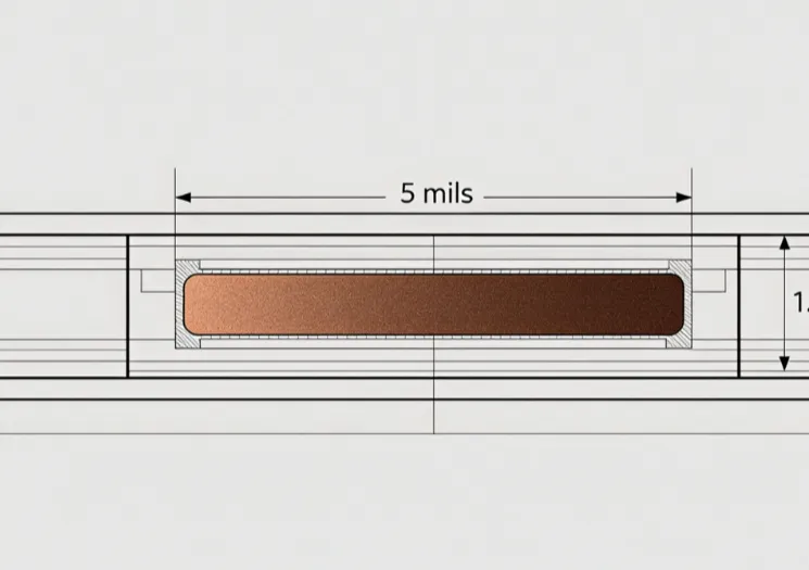
Trace width determines the cross-sectional area available for current flow in a copper conductor. Wider traces reduce electrical resistance and improve the overall current carrying capacity of the circuit. In power delivery PCB layouts, insufficient width causes voltage drops that affect downstream components and system performance. Copper thickness, typically specified in ounces per square foot, works together with width to set the final conductor area. Designers evaluate these factors early in the layout process to meet both functional and thermal constraints.
Industry standards guide the evaluation of these parameters during board design. IPC-2152 provides methods for assessing current-carrying capacity based on empirical data from various board configurations. Proper application of such guidance helps prevent overheating while optimizing board real estate.
Technical Principles Governing Trace Performance
Current flow through a copper trace generates heat according to the relationship between resistance and the square of the current. Resistance itself depends on the trace length, width, thickness, and the resistivity of the copper material. As current increases, temperature rise accelerates unless the trace geometry allows adequate heat dissipation into the surrounding dielectric and copper planes. Internal traces, surrounded by laminate on both sides, dissipate heat differently than external traces exposed to air or solder mask.
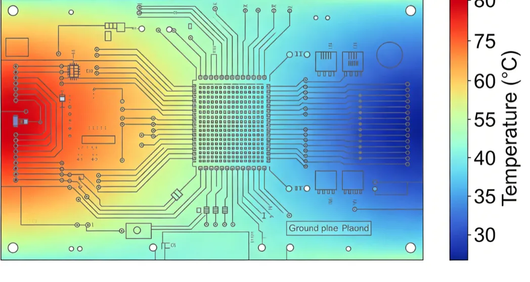
Several variables influence the final temperature rise for a given current. Board thickness, the presence of nearby copper pours or planes, and the thermal conductivity of the dielectric material all play roles. Trace location within the stackup further affects cooling efficiency. Engineers account for these interactions when determining appropriate dimensions for power traces.
Best Practices for Power Trace Sizing
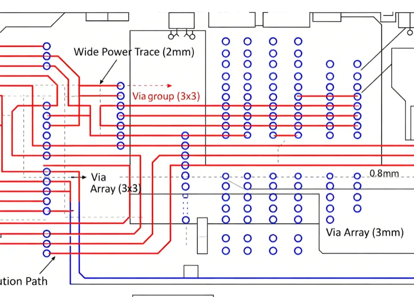
Designers begin by estimating the maximum continuous current each power net must carry under worst-case operating conditions. They then select an initial trace width based on copper weight and allowable temperature rise, iterating as needed after considering voltage drop requirements. Increasing copper thickness offers an alternative to widening traces when board space is limited. Multiple parallel traces or the use of copper pours can further enhance current capacity in high-power sections.
Verification against established guidelines ensures consistency across designs. IPC-2221 outlines general requirements for conductive materials and supports calculations related to temperature rise. Combining these approaches with simulation or prototype testing provides additional confidence before production.
Practical layout habits include maintaining adequate spacing between power traces and sensitive signal lines. Routing power paths with minimal length and avoiding sharp corners reduces inductance and improves current distribution. Placing vias strategically helps transfer current between layers while managing thermal paths.
Additional Considerations in Power Delivery Design
Stackup choices affect both electrical performance and thermal behavior of power traces. Thicker copper layers increase current capacity but may influence impedance control on adjacent signal layers. Dielectric materials with higher thermal conductivity assist in spreading heat away from traces. Designers review these interactions during the stackup definition phase to align with overall board requirements.
Environmental factors such as ambient temperature and airflow around the assembled board also influence allowable current levels. Enclosures that limit convection require more conservative trace sizing. System-level thermal analysis helps identify these constraints early.
Conclusion
Effective power delivery on PCBs requires deliberate selection of trace width in mils to achieve the necessary current carrying capacity. Understanding the interplay between geometry, material properties, and thermal dissipation enables reliable designs. Reference to established standards such as IPC-2152 supports consistent decision-making across projects. Structured evaluation of current needs, voltage drop, and temperature rise leads to optimized layouts that meet both performance and reliability goals.
FAQs
Q1: How does trace width in mils affect PCB trace width current performance?
A1: Trace width directly sets the conductor cross-section available for current flow. Wider traces in mils lower resistance and raise the current carrying capacity before temperature rise becomes excessive. Designers adjust width alongside copper thickness to satisfy power delivery PCB requirements while staying within thermal limits.
Q2: What factors determine current carrying capacity of a power trace?
A2: Current carrying capacity depends on trace width, copper thickness, layer location, and surrounding thermal environment. Standards such as IPC-2152 supply methods to evaluate these variables together. Proper sizing prevents overheating and maintains stable voltage delivery across the board.
Q3: Why is power trace sizing important in PCB design?
A3: Inadequate power trace sizing causes excessive heating, voltage drops, and reduced reliability in power delivery PCB applications. Appropriate dimensions ensure the trace can handle required currents without compromising other circuit functions. Early consideration during layout avoids costly revisions later.
Q4: How do engineers verify trace width for power applications?
A4: Engineers calculate initial dimensions from current requirements and then confirm performance through simulation or measurement. Guidelines in IPC-2221 and IPC-2152 provide reference points for temperature rise and conductor sizing. Final verification often includes prototype testing under expected load conditions.
References
IPC-2152 — Standard for Determining Current-Carrying Capacity in Printed Board Design. IPC, 2009
IPC-2221 — Generic Standard on Printed Board Design. IPC, 2023


