 ALLPCB


Why Reliable IoT PCB Performance Matters
IoT applications span industrial monitoring, smart infrastructure, and consumer electronics, where even brief interruptions affect data accuracy and system responsiveness. Power supply problems on PCBs can lead to voltage drops that cause microcontrollers to reset unexpectedly. Component failures often stem from thermal stress or mechanical vibration common in deployed devices. Addressing these issues early supports longer service life and reduces field maintenance needs.
Common PCB Signal Integrity Issues in IoT Designs
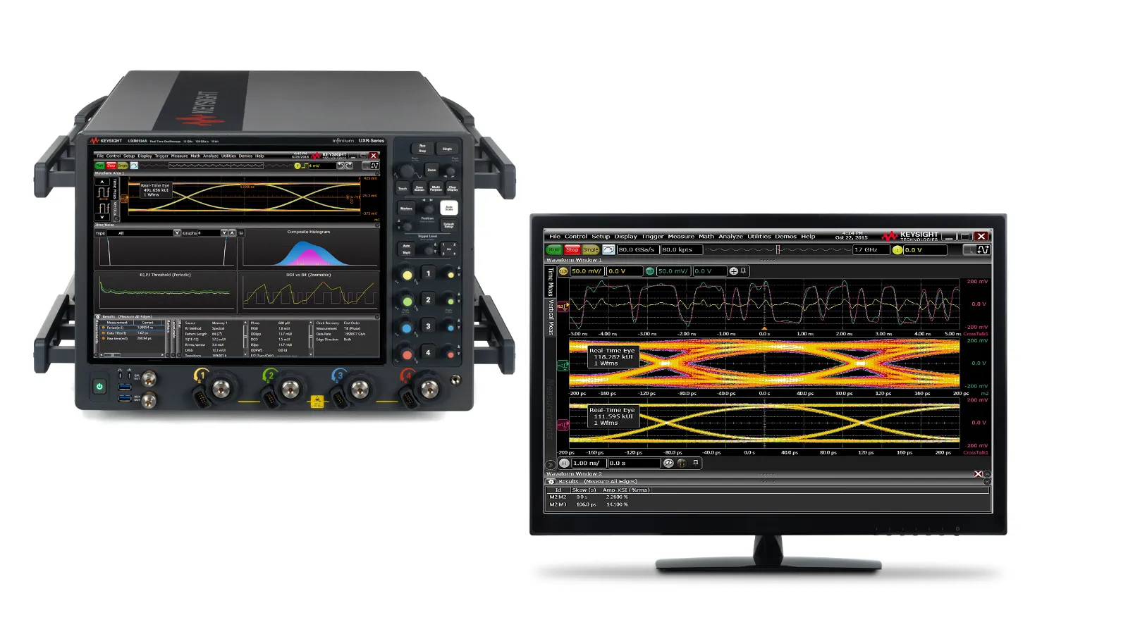
Signal integrity issues arise when high-speed traces experience reflections, crosstalk, or impedance mismatches. In IoT boards, dense layouts place RF traces near digital lines, increasing the chance of interference that corrupts sensor data. Ground plane discontinuities further degrade return paths and elevate noise levels. Engineers measure these effects using time-domain reflectometry or vector network analyzers during prototype validation.
Power Supply Problems on PCBs
Power delivery networks in IoT PCBs must supply stable voltages to multiple domains while managing current spikes from wireless transmissions. Decoupling capacitor placement and trace width directly influence voltage stability. Insufficient copper pour or poor via stitching can create inductive paths that amplify ripple. Thermal imaging during load testing reveals hot spots that indicate excessive resistance in power paths.
Component Failure Analysis Approaches
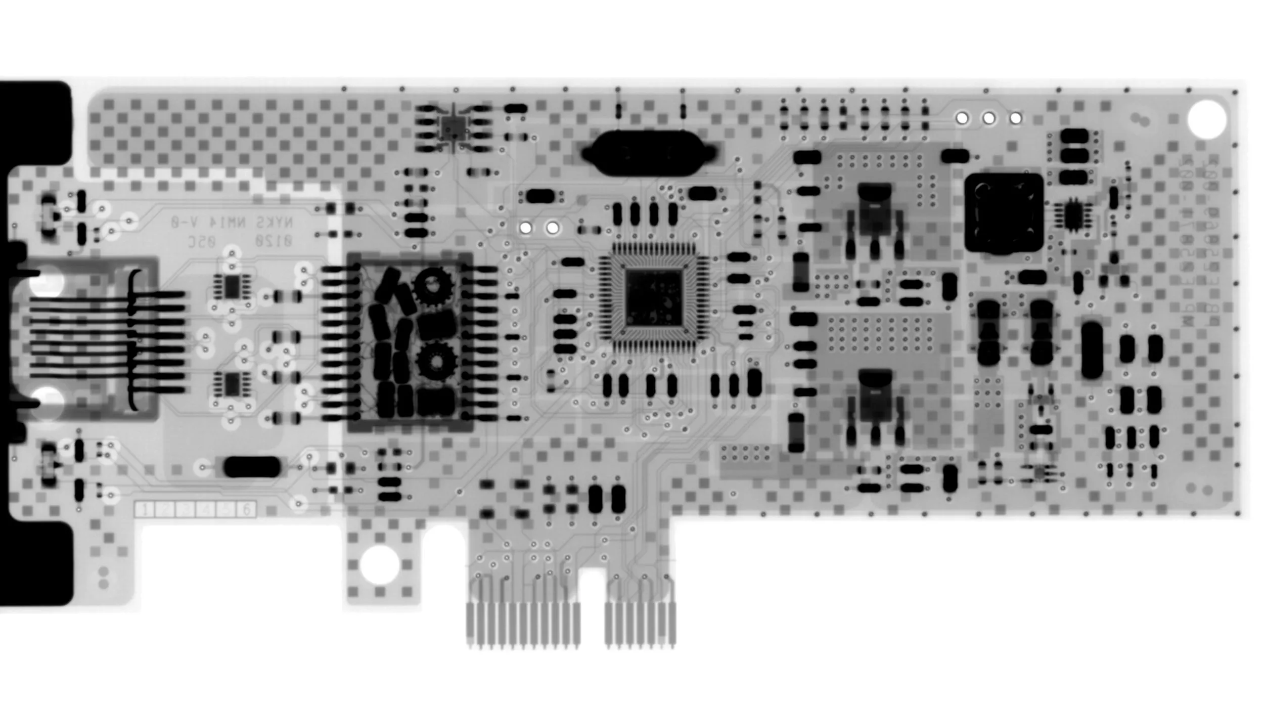
Component failure analysis begins with visual inspection followed by electrical testing to isolate open circuits, shorted pins, or parametric drift. Moisture ingress or thermal cycling often accelerates package cracking in surface-mount devices. X-ray imaging helps identify internal voids or delamination without destroying the assembly. Systematic root-cause evaluation distinguishes manufacturing defects from operational stresses.
PCB Testing Methods for Debugging IoT Boards
In-circuit testing verifies continuity and basic functionality of populated boards before firmware loading. Boundary scan techniques access device pins through JTAG interfaces to detect assembly faults quickly. Functional testing under simulated operating conditions confirms end-to-end performance, including wireless link stability. Automated optical inspection catches placement and soldering defects early in production.
Practical Solutions and Best Practices
Designers improve signal integrity by maintaining controlled impedance traces and providing continuous ground planes beneath critical signals. Power integrity benefits from star-topology distribution and adequate bypass capacitance near active devices. Thermal management practices include proper copper balancing and strategic component spacing to limit localized heating. Regular design reviews against established qualification criteria reduce the likelihood of recurring issues.
According to IPC-6012E, qualification testing establishes performance baselines for rigid printed boards used in demanding applications. Following IPC-A-600K acceptability criteria during inspection ensures consistent manufacturing quality.
Troubleshooting Workflow for IoT PCBs
A structured workflow starts with power-on checks to confirm voltage rails within specification. Oscilloscope probing then identifies noise or droop on critical nets. Firmware-level diagnostics log communication errors that point to signal integrity problems. Once isolated, targeted rework or layout revisions address the root cause before retesting the assembly.
Conclusion
Effective troubleshooting of IoT PCBs combines electrical measurements, visual inspection, and adherence to recognized industry practices. Engineers who apply systematic testing methods and address signal integrity, power delivery, and component reliability achieve more dependable device operation. Consistent application of these techniques supports the long-term performance expected in connected systems.
FAQs
Q1: What are the most frequent PCB signal integrity issues in IoT devices?
A1: Signal integrity issues in IoT PCBs commonly include impedance mismatches, crosstalk between traces, and ground return path disruptions that distort high-speed digital or RF signals. These problems often appear during wireless data transmission and can be identified through targeted oscilloscope measurements and layout review. Addressing them early prevents data corruption and improves overall device reliability.
Q2: How do power supply problems manifest on IoT PCBs?
A2: Power supply problems on PCBs typically appear as voltage ripple, sudden drops during peak loads, or excessive heating in distribution traces. Such issues disrupt microcontroller operation and wireless module performance. Proper decoupling strategies and adequate trace sizing help maintain stable rails across varying current demands.
Q3: What PCB testing methods support effective debugging of IoT assemblies?
A3: PCB testing methods such as in-circuit testing, boundary scan, and functional verification under load conditions allow engineers to locate assembly defects and performance shortfalls quickly. Combining these approaches with thermal imaging provides comprehensive insight into both electrical and thermal behavior during debugging sessions.
Q4: How is component failure analysis performed on IoT PCBs?
A4: Component failure analysis on IoT PCBs involves sequential steps of visual examination, electrical characterization, and non-destructive imaging to determine whether failures originate from manufacturing or operational stresses. This structured process guides corrective actions that enhance future board reliability.


