 ALLPCB


Introduction
In-circuit testing remains a foundational method for verifying electrical connections and component functionality on assembled printed circuit boards. Engineers and procurement teams often evaluate testing expenses closely because these costs directly influence overall project budgets and production timelines. Understanding the breakdown of in-circuit testing expenses helps teams allocate resources more effectively while maintaining product reliability. Factors such as fixture design, test program development, and equipment utilization all contribute to the total expenditure. A structured approach to budgeting for ICT supports consistent quality outcomes across multiple production runs.
What Is In-Circuit Testing and Why Cost Analysis Matters
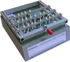
In-circuit testing applies a bed-of-nails fixture to access individual nodes on a populated board and measures parameters including resistance, capacitance, and voltage levels. This technique identifies manufacturing defects such as opens, shorts, and incorrect component values before functional testing begins. Cost analysis of in-circuit testing reveals how expenses accumulate from fixture fabrication, software programming, and ongoing maintenance activities. Teams that examine these elements can identify opportunities to streamline processes without compromising defect detection rates. Effective budgeting for ICT therefore supports both quality control objectives and financial planning requirements in electronics manufacturing environments.
Key Factors Influencing ICT Costs
Fixture development represents one of the primary drivers of in-circuit testing expenses because custom probes and alignment mechanisms must match the specific board layout. Programming the test sequence requires skilled engineering time to define measurement points and tolerance limits for each component. Equipment depreciation and calibration schedules add recurring costs that scale with production volume. Board complexity, including the number of nodes and component density, further increases both fixture and program development efforts. Organizations that track these variables gain clearer visibility into total testing expenditures and can forecast requirements for future projects more accurately.
Adherence to established industry standards helps maintain consistency in test coverage and documentation practices. Engineers often reference IPC guidelines when defining acceptance criteria for electrical measurements performed during in-circuit testing. This alignment reduces the likelihood of rework caused by ambiguous specifications and supports repeatable results across different production batches.
Technical Principles Behind Cost Variations
The electrical interface between the fixture and the board determines measurement accuracy and influences how much time each test cycle requires. Probe contact resistance and signal integrity considerations become more critical as node counts rise, directly affecting program execution duration. Test coverage decisions also play a role because expanding the number of measured parameters increases both programming effort and fixture complexity. Engineers balance these technical requirements against available budget allocations by prioritizing high-risk defect categories. Structured analysis of these mechanisms allows teams to optimize test sequences while preserving essential verification steps.
Practical Solutions and Cost-Effective PCB Testing Strategies
Standardizing fixture designs across similar board families reduces fabrication expenses by reusing mechanical components and probe layouts. Modular programming approaches enable reuse of test routines for common components, shortening development cycles for subsequent projects. Scheduling preventive maintenance on test equipment minimizes unplanned downtime that can inflate operational costs. Early involvement of test engineers during board layout review helps identify accessibility issues before fixture production begins. These coordinated efforts contribute to more predictable budgeting for ICT across multiple product generations.
Related Reading: Cost-Effective ICT Testing: Strategies for Optimizing Test Fixture Design
Additional Strategies for Reducing ICT Testing Expenses
Batch processing of boards with compatible test requirements improves equipment utilization rates and lowers per-unit costs. Periodic review of test coverage against actual defect data allows removal of redundant measurements that add little value. Training programs for operators and programmers enhance efficiency and reduce errors that lead to repeated test cycles. Collaboration between design and test teams during schematic capture ensures adequate test point placement without excessive board real estate usage. Implementing these measures supports sustained cost control while preserving the diagnostic benefits of in-circuit testing.
Related Reading: Unlocking Efficiency: How In Circuit Testing Optimizes PCB Assembly
Conclusion
Systematic examination of in-circuit testing cost factors enables engineering teams to develop realistic budgets and identify meaningful reduction opportunities. Attention to fixture design, program development, and equipment utilization produces measurable improvements in testing economics. Integration of industry standards into test planning further strengthens process reliability. Organizations that apply these principles consistently achieve better alignment between quality goals and financial constraints. Continued refinement of cost-effective PCB testing strategies supports long-term competitiveness in electronics production.
FAQs
Q1: What elements contribute to an in-circuit testing cost breakdown?
A1: An in-circuit testing cost breakdown typically includes fixture fabrication, test program development, equipment calibration, and operator time. Each of these elements scales with board complexity and production volume. Engineers evaluate these components to create accurate forecasts and identify areas where expenses can be moderated. Understanding the full breakdown supports more informed decisions during project planning.
Q2: Which ICT cost factors have the greatest impact on overall expenses?
A2: ICT cost factors such as fixture customization and test sequence length often exert the strongest influence on total spending. Higher node counts and denser component placement increase both mechanical and programming demands. Teams that quantify these influences can prioritize design adjustments that yield the largest savings while maintaining required test coverage.
Q3: How can teams implement reducing ICT testing expenses without sacrificing quality?
A3: Reducing ICT testing expenses begins with early collaboration between design and test engineers to optimize node accessibility. Reuse of standardized fixture modules and test routines across similar products further lowers development costs. Regular review of test data helps eliminate unnecessary measurements, preserving defect detection capability while controlling expenditures.
Q4: What approaches support effective budgeting for ICT across multiple projects?
A4: Budgeting for ICT benefits from historical data collection on fixture and program costs for comparable boards. Forecasting tools that account for board size, component count, and expected volume improve accuracy. Consistent application of these methods allows procurement and engineering teams to allocate resources efficiently throughout the product lifecycle.
References
IPC-A-610G — Acceptability of Electronic Assemblies. IPC, 2017
IPC-6012E — Qualification and Performance Specification for Rigid Printed Boards. IPC, 2017
JEDEC J-STD-020E — Moisture/Reflow Sensitivity Classification. JEDEC, 2014


