ALLPCB


Introduction
Surface mount technology dominates modern PCB assembly, where precise solder paste deposition sets the foundation for reliable solder joints. The stencil acts as the critical interface, transferring exact volumes of paste through apertures aligned to component pads. Selecting the appropriate stencil material influences print consistency, defect rates like bridging or starving, and long-term production efficiency. Stainless steel stencils and nickel stencils represent the primary options, each offering distinct stencil properties that suit different assembly challenges. Engineers must evaluate factors such as aperture quality, durability, and compatibility with fine-pitch components to make informed material selection decisions. This guide provides practical insights into comparing these materials, drawing from industry-established practices to optimize PCB assembly outcomes.
Stainless steel stencils excel in high-volume scenarios due to their robustness, while nickel stencils shine in precision-demanding applications. Poor material choice often leads to troubleshooting headaches, such as inconsistent paste release or accelerated wear. By understanding stencil material characteristics, teams can reduce rework and enhance first-pass yields. This article explores technical differences, selection criteria, and real-world guidance tailored for electric engineers handling diverse PCB assembly needs.
What Are SMT Stencils and Why Does Material Selection Matter?
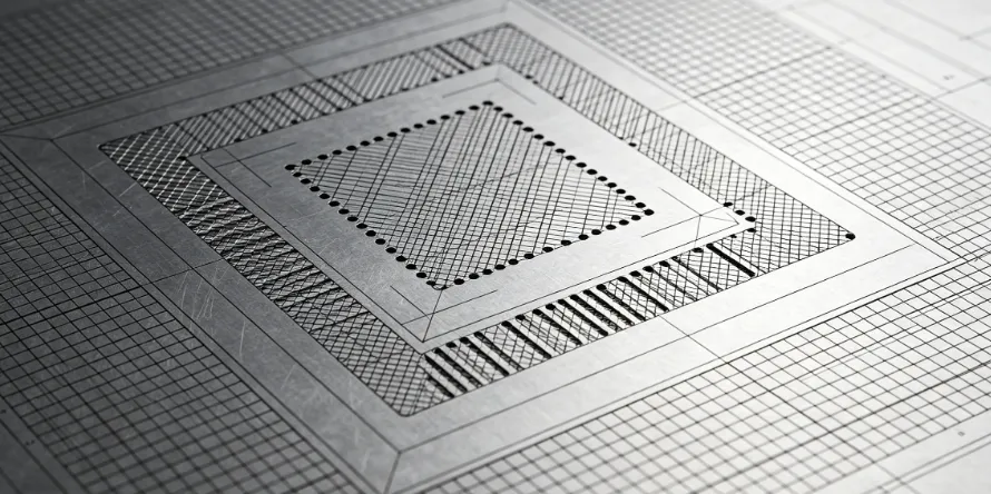
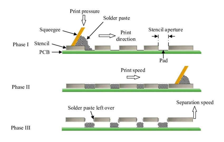
SMT stencils consist of thin metal foils with precisely cut apertures that mirror PCB pad layouts. During printing, the stencil contacts the board, and squeegees force solder paste into these openings, creating uniform deposits for reflow soldering. Material selection directly affects aperture wall finish, paste transfer efficiency, and stencil lifespan under repeated cycles. IPC-7525C identifies stainless steel and nickel as typical foil materials, emphasizing their role in achieving consistent performance across production runs. Incorrect choices amplify risks like insufficient paste volume on fine features or excessive residue buildup.
The relevance intensifies with shrinking component pitches, where stencil properties dictate assembly success. Stainless steel suits broader applications through cost-effective fabrication, but nickel addresses limitations in paste release for tighter geometries. Material impacts extend to cleaning frequency, tension stability, and compatibility with automated printers. Engineers prioritizing yield must align stencil material with board complexity, paste rheology, and volume expectations. Neglecting this step invites variability that cascades into reflow defects and reliability issues.
Key Stencil Properties Influencing PCB Assembly
Stencil properties encompass mechanical strength, surface finish, chemical resistance, and dimensional stability. Aperture walls must promote clean paste release to avoid bridging during printing. Durability ensures the stencil withstands thousands of prints without deformation or clogging. Stainless steel provides high tensile strength and wear resistance, ideal for demanding environments. Nickel offers superior smoothness from electroforming, minimizing paste adhesion on intricate features.
Fabrication methods shape these properties further. Laser-cutting stainless steel yields straight walls but introduces minor roughness, while electroforming nickel produces tapered, mirror-like surfaces. Tension control prevents warping, crucial for fiducial alignment in high-precision setups. Chemical resistance guards against paste solvents during cleaning. Collectively, these traits determine how well the stencil integrates into the PCB assembly workflow, influencing throughput and quality control metrics.
Stainless Steel Stencils: Strengths and Ideal Use Cases
Stainless steel stencils dominate due to their balance of affordability and robustness in PCB assembly. Fabricated via laser cutting or etching, they deliver reliable performance for standard pitch components. The material's inherent hardness resists deformation from squeegee pressure, supporting extended production runs. Engineers appreciate its ease of handling and compatibility with electropolishing to refine surface properties. This makes stainless steel a go-to for prototypes transitioning to volume manufacturing.
Practical advantages include quick turnaround times and lower upfront costs compared to alternatives. In troubleshooting, stainless steel holds up well against abrasion from type 4 or 5 solder pastes. However, rougher walls may require optimized printing parameters to ensure consistent release. For assemblies with pitches above typical thresholds, pairing with nano-coatings enhances longevity. Overall, stainless steel streamlines material selection when precision demands remain moderate.
Nickel Stencils: Precision for Challenging Applications
Electroformed nickel stencils target fine-pitch PCB assembly where paste release precision is paramount. The process builds apertures atom-by-atom, resulting in ultra-smooth, tapered walls that reduce residue retention. This property excels with micro-BGAs or 0201 components, minimizing defects like head-in-pillow. Nickel's corrosion resistance suits harsh cleaning regimens, maintaining performance over cycles. Engineers select it when standard stainless steel falls short in transfer efficiency.
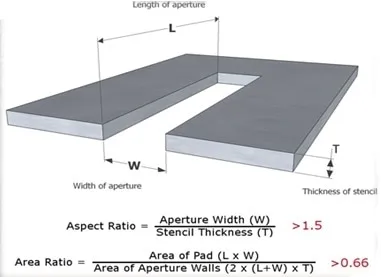
Drawbacks center on higher fabrication complexity and cost, with longer lead times for custom designs. Brittleness in thicker foils demands careful tensioning to avoid cracks. Yet, for troubleshooting ultra-fine features, nickel's mirror finish often justifies the investment. Compliance with IPC-7525C guidelines reinforces its use in designs requiring area ratios above standard benchmarks. Nickel empowers reliable printing in high-density boards, where every micron counts.
Stainless Steel vs. Nickel: A Direct Comparison
Aperture Wall Finish — Stainless Steel: Straighter, moderately rough (laser-cut). Nickel: Ultra-smooth, tapered (electroformed).
Paste Release — Stainless Steel: Good with polishing; parameter-dependent. Nickel: Excellent, minimal adhesion.
Durability — Stainless Steel: High wear resistance for volume runs. Nickel: Strong corrosion resistance; may be volume-limited by process and brittleness in thicker foils.
Cost — Stainless Steel: Lower, faster production. Nickel: Higher, specialized process.
Best For — Stainless Steel: Standard pitches, high-volume. Nickel: Fine-pitch, precision applications.
This comparison highlights core stencil properties guiding material selection. Stainless steel prioritizes economy and toughness, while nickel focuses on finesse. J-STD-001J criteria for soldered joints underscore how material choice affects joint formation. Use it to match assembly needs swiftly.
Best Practices for Stencil Material Selection in PCB Assembly
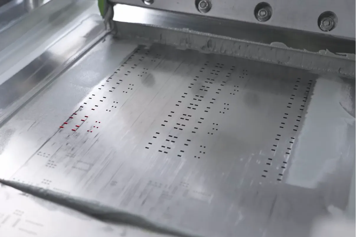
Assess component pitch first: opt for nickel below fine thresholds to leverage smooth release. For coarser layouts, stainless steel suffices with post-processing like electropolishing. Factor in production volume, as stainless steel's durability scales better for thousands of prints. Test paste compatibility through trial runs, adjusting squeegee speed and pressure accordingly. Maintain stencil tension per manufacturer specs to prevent misalignment.
Incorporate IPC-7525C recommendations for aperture design alongside material. Prototype with stainless steel, then scale to nickel if yields lag on fine features. Regular cleaning protocols extend life, using approved solvents to preserve surface integrity. Document printing parameters for repeatability across shifts. This systematic approach minimizes troubleshooting and aligns stencil properties with overall PCB assembly goals.
Troubleshooting Common Stencil Issues by Material
Insufficient paste deposit often signals rough walls in stainless steel; refine with nano-coatings or slower print speeds. Bridging plagues fine-pitch boards, where nickel's smoothness resolves adhesion issues effectively. Excessive wear appears as aperture enlargement, favoring stainless steel's hardness for abrasive pastes. Warping from improper storage affects both, but nickel's flexibility aids recovery.
Inspect under magnification post-cleaning to spot residue traps. If release falters, verify alignment and consider material switch. Poor tension leads to smearing, resolvable by frame adjustments. Log defect patterns to correlate with stencil properties, enabling proactive swaps. These steps restore process control swiftly.
Conclusion
Choosing between stainless steel stencils and nickel stencils hinges on balancing precision, durability, and cost for specific PCB assembly demands. Stainless steel offers versatile, economical solutions for most runs, while nickel tackles fine-pitch challenges with superior release. Key stencil properties like wall finish and wear resistance drive decisions, supported by standards such as IPC-7525C. Practical evaluation through trials ensures optimal material selection, reducing defects and boosting yields. Engineers equipped with this knowledge can troubleshoot effectively and streamline production. Prioritize alignment with board complexity for sustained assembly excellence.
FAQs
Q1: What are the primary stencil properties to evaluate during material selection for PCB assembly?
A1: Stencil properties such as aperture wall smoothness, durability, and paste release performance top the list. Stainless steel provides robust wear resistance for high-volume use, while nickel excels in smooth finishes for fine-pitch reliability. Consider fabrication method and cleaning compatibility to match assembly needs. This evaluation prevents common print defects and ensures consistent solder joints.
Q2: When should electric engineers choose nickel stencils over stainless steel for PCB assembly?
A2: Opt for nickel stencils in fine-pitch designs where superior paste release is critical, such as micro-BGAs. Their electroformed walls minimize adhesion, reducing bridging risks absent in laser-cut stainless steel. Reserve stainless steel for coarser pitches and volume production. Trial prints confirm the switch boosts yields without excessive cost.
Q3: How do stainless steel stencils perform in high-volume PCB assembly compared to nickel?
A3: Stainless steel stencils thrive in high-volume PCB assembly due to their hardness and lower cost, enduring repeated cycles with minimal deformation. Nickel suits precision but may limit throughput from fabrication delays. Enhance stainless steel with polishing for better release. Both align with IPC-7525C for reliable performance.
Q4: What role does stencil material play in troubleshooting solder paste printing defects?
A4: Stencil material directly influences defects like starving or bridging through properties like surface finish. Rough stainless steel walls may trap paste, resolvable by parameters or coatings, while nickel prevents this inherently. Inspect and log issues to guide swaps. Proper selection upfront cuts troubleshooting time significantly.
References
IPC-7525C — Stencil Design Guidelines. IPC, 2021
IPC J-STD-001J — Requirements for Soldered Electrical and Electronic Assemblies. IPC, 2024