 ALLPCB


Introduction
In PCB design, determining the ideal line width tolerance ensures reliable performance under electrical and thermal stresses. Electrical engineers must balance manufacturing capabilities with functional requirements to avoid issues like overheating or signal degradation. Line width tolerance directly influences current handling, impedance control, and overall board yield. This article outlines structured methods for PCB trace width calculation, incorporating factors such as current calculation and impedance calculation. By following these principles, designers can optimize traces for their specific project needs. Understanding these calculations helps prevent costly redesigns and enhances product reliability.
What Is Line Width Tolerance and Why It Matters
Line width tolerance refers to the permissible variation in the fabricated width of PCB traces from the nominal design value. Manufacturers specify this as a percentage or absolute value, often tied to production class and process controls. For instance, deviations occur due to etching undercuts, copper plating variations, and exposure inconsistencies during photolithography. In high-reliability applications, tight tolerances prevent excessive resistance increases or impedance mismatches that could lead to failures.
This parameter matters because trace width directly affects electrical performance. Narrower traces risk higher resistance and heat buildup, while wider ones may cause crosstalk or routing congestion. Proper tolerance selection aligns design intent with fabrication reality, ensuring compliance with performance specs. Engineers targeting high-speed signals or power delivery must prioritize it to maintain signal integrity and thermal margins.
Key Technical Principles Behind Line Width Determination
PCB trace width primarily derives from current carrying capacity requirements. The relationship between current, width, copper thickness, and allowable temperature rise forms the core of current calculation. Thicker copper allows narrower widths for the same current, but external traces dissipate heat better than internal ones. Standards like IPC-2152 provide charts and models accounting for these variables, replacing older IPC-2221 guidelines for more accurate predictions.
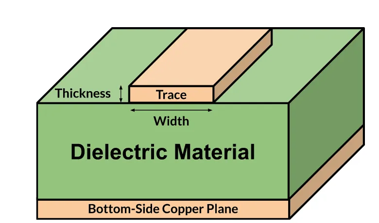
Impedance calculation introduces another dimension, especially for controlled impedance designs. Characteristic impedance depends on trace width, dielectric height, and material properties in microstrip or stripline configurations. Wider traces reduce impedance, while narrower ones increase it, affecting signal reflection and timing. Engineers use field solver equations or approximations to iterate widths until target values, such as 50 ohms single-ended, are met.
Manufacturing introduces tolerance as a statistical variation around the nominal width. Etching processes typically yield tolerances of 10 to 20 percent, with minimum widths enforced to guarantee functionality. IPC-6012 outlines performance specifications, including conductor width minima at 80 percent of design for certain classes. These principles ensure traces meet both electrical and producibility criteria without overdesign.
Factors Influencing Trace Width and Tolerance
Several stackup and material factors interplay with line width selection. Dielectric constant and thickness primarily drive impedance, requiring width adjustments for consistent performance across layers. Copper weight, from 1 oz to 2 oz per square foot, scales current capacity linearly but impacts etching precision. Higher frequencies demand finer widths for controlled impedance, amplifying tolerance sensitivity.
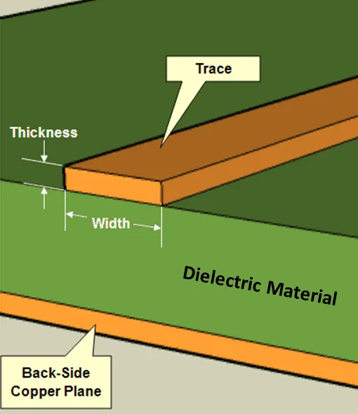
Thermal management adds complexity, as current calculation must consider ambient conditions and board population density. Traces near heat sources or in dense arrays experience reduced capacity due to mutual heating. Tolerance margins protect against worst-case narrowing, preserving derated current limits. Engineers simulate these via thermal models integrated into design flows.
Process class defines tolerance expectations, with Class 3 boards demanding tighter controls than Class 2. Higher classes reduce allowable deviations, increasing costs but enhancing reliability. Fabricators provide capability matrices linking minimum widths to spacing rules. Selecting the right class aligns project risk with budget constraints.
Practical Steps for PCB Trace Width Calculation
Begin with project requirements: identify maximum current, target impedance, frequency, and class. For power traces, perform current calculation using IPC-2152 models, inputting copper thickness and temperature rise limit. This yields nominal width; add 20 percent margin for tolerance to ensure minimum fabricated width meets needs.
For signal integrity, run impedance calculation iteratively. Start with stackup parameters, compute required width, then verify with field solvers. Adjust for tolerance by designing to the upper spec limit, ensuring even narrowed traces hit impedance targets. Combine both via multi-objective optimization in design tools.
Leverage PCB design software for integrated analysis. These platforms embed calculators for trace width, current, and impedance, simulating full layouts. Export stackups to fabricators for impedance verification. Online calculators offer quick preliminary checks during schematic stages.

Specify tolerances explicitly on fabrication drawings, referencing applicable standards. Request production panels with test coupons for width verification. Post-fabrication, measure traces via automated optical inspection to confirm compliance. This closed-loop process refines future designs.
Best Practices for Incorporating Tolerance in Design
Adopt a conservative approach by designing traces wider than minimum calculations suggest. Factor in aging effects like electromigration, which narrow traces over time under high current density. Limit densities to 80 percent of capacity for longevity. Use via stitching for heat spreading on power planes.
For high-speed designs, prioritize impedance over current where conflicting. Tolerance-controlled etching processes, like direct imaging, tighten variations to under 10 percent. Collaborate early with fabricators to match capabilities. Simulate tolerance stacks in Monte Carlo analyses for yield prediction.
Document assumptions in design reviews, including class and margins. Transition to higher copper weights for compact boards, recalculating widths accordingly. Regular audits of supplier data ensure consistency. These practices minimize risks across production volumes.
Case Study: Optimizing a High-Current Automotive Controller
Consider a multilayer board for an automotive power controller handling 10A peaks. Initial current calculation per IPC-2152 suggested 100 mil external traces at 1 oz copper for 20C rise. Impedance needs for control signals required 6 mil widths at 100 ohms differential. Tolerance analysis revealed 15 percent variation risk, prompting 15 mil power traces to guarantee capacity. Simulations confirmed impedance stability post-etching. Production test coupons validated widths at 95 percent nominal average. Final boards passed thermal cycling without failures, demonstrating tolerance integration benefits.
Conclusion
Calculating ideal line width tolerance integrates current calculation, impedance calculation, and manufacturing realities for robust PCBs. Engineers achieve this through standards-guided nominal sizing, margin application, and verification. PCB design software and online calculators streamline iterations, enhancing accuracy. Prioritizing these steps ensures high yield and performance. Adopt structured workflows to future-proof projects against evolving demands.
FAQs
Q1: How do you perform PCB trace width calculation for power delivery?
A1: PCB trace width calculation starts with current requirements, copper thickness, and temperature rise limits using IPC-2152 models. Input these into design software or online calculators to get nominal width. Add tolerance margin, typically 20 percent, to account for etching variations. Verify with thermal simulations for dense layouts. This ensures safe operation without excessive heating.
Q2: What role does impedance calculation play in trace width selection?
A2: Impedance calculation determines trace width based on stackup, dielectric, and target values like 50 ohms. Wider traces lower impedance; narrower ones raise it. Incorporate manufacturing tolerance by designing to the maximum width spec. Use field solvers in PCB design software for precision. This maintains signal integrity in high-speed applications.
Q3: Why include tolerance in current calculation for PCB traces?
A3: Tolerance in current calculation compensates for fabricated widths narrower than design, preserving capacity. Standards like IPC-6012 specify minima around 80 percent nominal. Design with margins to derate for safety. Online calculators often include tolerance options. This prevents overheating in real-world use.
Q4: Can online calculators replace PCB design software for trace analysis?
A4: Online calculators provide quick estimates for PCB trace width calculation and impedance but lack full layout context. PCB design software offers integrated simulations with stackups and parasitics. Use calculators for initials, software for finals. Both aid tolerance assessment effectively.
References
IPC-2152 — Standard for Determining Current Carrying Capacity in Printed Board Design. IPC, 2009
IPC-6012E — Qualification and Performance Specification for Rigid Printed Boards. IPC, 2015
IPC-A-600K — Acceptability of Printed Boards. IPC, 2020





