 ALLPCB


Why EMI/EMC Compliance Matters in 12-Layer Designs
Complex electronic products must satisfy emission and immunity standards to operate reliably in shared electromagnetic environments. In a 12-layer stackup, the additional layers enable dedicated power and ground planes that reduce loop inductance and improve return paths for high-frequency currents. Failure to control noise sources can result in functional failures, regulatory non-compliance, or costly redesign cycles during product qualification. Engineers therefore integrate shielding and grounding considerations from the initial stackup definition through final layout verification.
Technical Principles of Grounding in Multilayer Boards
Effective grounding begins with continuous, low-impedance reference planes that serve as return paths for signal currents. In a typical 12-layer configuration, multiple ground planes are distributed to separate analog, digital, and power domains while maintaining overall board rigidity. Stitching vias connect these planes at frequent intervals to minimize slot antennas and maintain equipotential surfaces across the board. This approach reduces voltage differences that would otherwise radiate energy or couple noise between layers.
Shielding techniques complement grounding by containing electromagnetic fields within designated regions. Copper pours on outer layers or internal shield layers create Faraday cage effects when connected to the ground system at multiple points. For high-frequency signals, the shield effectiveness depends on the continuity of the conductive enclosure and the quality of its connection to the reference plane. Proper implementation limits both radiated emissions from internal traces and susceptibility to external fields.
Layer Stackup Considerations for Noise Control
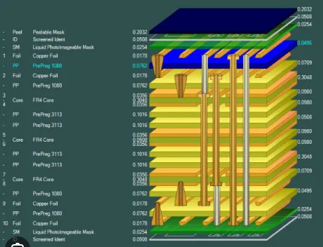
A well-planned 12-layer stackup positions signal layers adjacent to ground planes to provide controlled impedance and tight return paths. Power planes are typically placed next to ground planes to form low-inductance decoupling structures. Symmetric arrangements around the board center help control warpage during thermal cycling. Such configurations inherently support lower radiated emissions by shortening current loops and reducing the effective antenna size of traces and vias.
Practical Shielding and Grounding Techniques
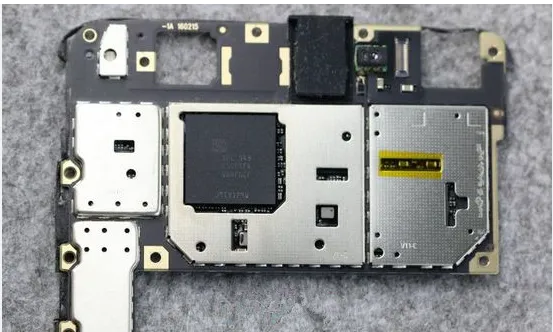
Designers begin by allocating specific layers for continuous ground planes and ensuring that all high-speed signals reference these planes directly. Ground vias are placed liberally around board edges and near connectors to create a low-impedance perimeter shield. Where enclosure-level shielding is required, board-level shield cans or conductive gaskets connect to multiple ground points to avoid creating resonant cavities.
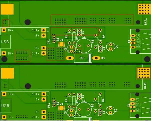
Decoupling capacitors are positioned as close as possible to integrated circuit power pins, with vias connecting to both power and ground planes. This placement minimizes the inductance of the local power distribution network and reduces conducted emissions along power traces. In regions with dense routing, ground pours on signal layers fill unused areas and connect to the primary ground planes through vias spaced at intervals no greater than one-twentieth of the wavelength of concern.
Best Practices for Emission Reduction
Trace routing follows the shortest possible paths while maintaining consistent reference to the nearest ground plane. Differential pairs are routed with controlled spacing and length matching to cancel common-mode currents that contribute to radiated emissions. Clock and periodic signals receive additional attention through guard traces or dedicated ground return vias placed adjacent to signal vias.
Board edges receive particular focus because discontinuities in ground planes can act as slot radiators. Continuous copper on outer layers connected to internal ground planes through edge vias helps suppress these effects. When mixed-signal sections coexist on the same board, separate ground regions connected at a single low-frequency point or through a controlled impedance bridge prevent noise coupling between domains.
Verification and Iteration
Post-layout simulation of radiated and conducted emissions provides early indication of compliance risk before fabrication. Three-dimensional electromagnetic solvers model the interaction between traces, planes, and any shield structures. Measured results from prototype boards then validate the models and guide refinements such as additional stitching vias or adjusted component placement.
Conclusion
Systematic application of continuous ground planes, strategic via stitching, and enclosure shielding enables 12-layer PCBs to meet stringent EMI/EMC requirements. These techniques reduce both radiated and conducted emissions while preserving signal integrity across high-speed interfaces. Early integration of grounding and shielding decisions into the stackup and layout process minimizes iteration and supports reliable product certification.
FAQs
Q1: How does a 12-layer PCB improve EMI shielding compared with fewer layers?
A1: Additional layers allow dedicated ground planes that provide low-inductance return paths and enable internal shielding structures. This arrangement shortens current loops and reduces the radiation efficiency of traces and vias, directly supporting lower radiated emissions in 12-layer PCB EMI shielding applications.
Q2: What grounding techniques are most effective for controlling 12-layer PCB EMC grounding performance?
A2: Continuous reference planes combined with frequent stitching vias maintain equipotential surfaces and minimize voltage gradients. These practices, together with careful separation of analog and digital domains, reduce both conducted and radiated noise in 12-layer PCB EMC grounding designs.
Q3: Which layout choices help reduce 12-layer PCB noise reduction challenges?
A3: Placing high-speed signals adjacent to ground planes, using controlled-impedance routing, and filling unused areas with connected copper pours limit noise coupling. Proper decoupling capacitor placement and edge via stitching further contribute to effective 12-layer PCB noise reduction.
Q4: How can designers address 12-layer PCB radiated emissions and conducted emissions simultaneously?
A4: A combination of solid ground planes, shield cans connected at multiple points, and filtered power entry points targets both emission types. Simulation followed by prototype measurement confirms that these measures keep 12-layer PCB radiated emissions and conducted emissions within acceptable limits.
References
IPC-6012E — Qualification and Performance Specification for Rigid Printed Boards. IPC, 2017
IEC 61000-4-3 — Testing and Measurement Techniques — Radiated, Radio-Frequency, Electromagnetic Field Immunity Test. IEC, 2020
IPC-A-600K — Acceptability of Printed Boards. IPC, 2020





