 ALLPCB


Standard total PCB thickness plays a central role in many beginner and intermediate electronics projects. Hobbyists often select boards that follow widely accepted dimensions because these sizes align with common component footprints, enclosure designs, and assembly methods. Working with the standard thickness simplifies layout decisions and reduces the chance of mechanical fit issues during prototyping. This approach supports reliable results without requiring specialized equipment or advanced manufacturing knowledge.
What Is Standard PCB Thickness and Why It Matters for Hobbyists
The industry recognizes 1.57 mm, or approximately 0.062 inches, as the conventional total thickness for rigid printed circuit boards. This dimension includes the core dielectric material plus copper foil on one or both sides. For electronic hobbyists, this thickness provides a practical balance between mechanical rigidity and ease of handling during DIY assembly. Boards at this thickness fit standard card-edge connectors and many off-the-shelf enclosures without modification.
Using the standard thickness supports consistent thermal performance during soldering and helps maintain planarity across the board surface. Deviations from this norm can introduce challenges such as excessive flexing in larger boards or difficulties when mounting through-hole components. Hobbyists benefit from selecting this thickness because it matches the specifications used in most educational kits and open-source hardware designs.
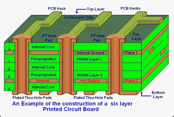
Technical Principles Behind Standard PCB Thickness
Total thickness is determined by the sum of the insulating substrate, typically FR-4 epoxy glass, and the copper layers applied to its surfaces. The core thickness is chosen during manufacturing to achieve the target overall dimension after copper plating and solder mask application. Industry specifications define acceptable tolerances around the nominal value to ensure interchangeability across different production runs.
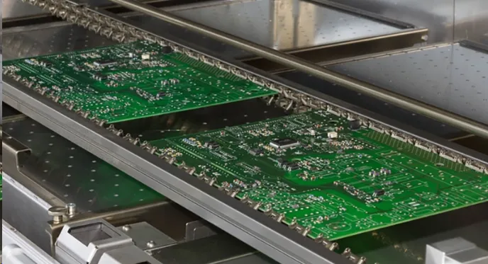
Warpage and twist become more noticeable when boards deviate significantly from the standard thickness, especially under temperature changes during reflow or wave soldering. IPC-6012E outlines qualification requirements that include dimensional stability for rigid boards, helping manufacturers deliver consistent products. Hobbyists working on DIY PCB projects notice that standard-thickness boards resist bending better than thinner variants when populated with heavier components.
Copper weight also influences the final thickness, yet the overall board dimension remains the controlling factor for most mechanical considerations. Thicker copper increases current-carrying capacity but adds only a small increment to the total height when the core stays at the conventional value.
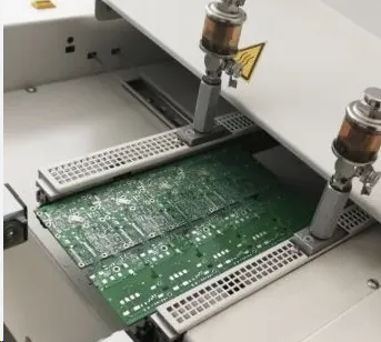
Practical Solutions and Best Practices for Easy PCB Projects
Hobbyists can start most simple projects by ordering or fabricating boards at the standard total thickness. This choice works well for LED arrays, sensor interfaces, power distribution modules, and small microcontroller carriers. When laying out the board, maintain adequate spacing between traces and use standard drill sizes that match common component leads.
During assembly, support the board on a flat surface to prevent flexing while soldering. Standard thickness allows the use of ordinary hand tools and soldering stations without special fixtures. For double-sided designs, ensure that plated through-holes maintain sufficient annular ring width to meet basic reliability expectations.
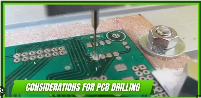
When cutting or routing boards, follow the grain direction of the fiberglass to minimize edge delamination. Hobbyists often find that standard-thickness material drills cleanly with carbide bits at moderate speeds. After etching or milling, inspect the surface for uniform copper removal and verify that the overall thickness remains within a few percent of the nominal value.
Troubleshooting Common Issues with PCB Thickness in Hobby Projects
If a project experiences intermittent connections after assembly, check whether the board has flexed during handling and caused stress on solder joints. Standard thickness reduces this risk compared with thinner materials. When components sit unevenly, verify that the board remains flat before and after soldering by placing it on a known flat reference.
Excessive heat during soldering can cause localized expansion differences; allowing the board to cool gradually helps preserve planarity. For projects that require repeated insertion into connectors, the standard thickness provides the necessary stiffness to avoid deformation over time.
Conclusion
Selecting the standard total PCB thickness simplifies many aspects of electronic hobbyist work. It aligns with common component packages, supports straightforward mechanical integration, and follows established industry expectations for dimensional consistency. By focusing on this conventional dimension, hobbyists achieve reliable prototypes with minimal trial and error.
FAQs
Q1: What is the standard PCB thickness used in most easy PCB projects?
A1: The conventional thickness of 1.57 mm provides a reliable starting point for DIY PCB work because it balances rigidity and ease of handling while matching widely available components and enclosures.
Q2: Why should PCB thickness for hobbyists stay close to the industry standard?
A2: Staying near the standard thickness helps avoid mechanical issues such as excessive flexing or poor fit with connectors, allowing hobbyists to focus on circuit function rather than custom fixturing.
Q3: How does standard PCB thickness affect DIY PCB assembly?
A3: Standard thickness supports clean drilling, even soldering, and good planarity, reducing the likelihood of warped boards or stressed joints during typical hobbyist soldering and testing procedures.
Q4: Can hobbyists use non-standard thicknesses for simple projects?
A4: Non-standard thicknesses are possible but often require extra care with support during assembly and may limit compatibility with standard connectors or cases, making the conventional thickness preferable for most beginners.
References
IPC-6012E — Qualification and Performance Specification for Rigid Printed Boards. IPC, 2017
IPC-A-600K — Acceptability of Printed Boards. IPC, 2020





