 ALLPCB


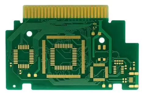
Hard gold plating provides a durable, corrosion-resistant surface finish ideal for high-wear areas in electronics projects. Hobbyists often apply it to edge connectors, switch contacts, or test points on custom PCBs to improve longevity and maintain low contact resistance during repeated insertions or mating cycles. This finish consists of a thin layer of hardened gold deposited electrolytically over a nickel barrier layer on copper traces or pads. The nickel prevents diffusion of copper into the gold while the gold delivers excellent conductivity and wear resistance. For home use, the process remains accessible with basic electroplating setups, though it requires careful attention to surface preparation and safety protocols to achieve reliable results.
Why Hard Gold Plating Matters for Electronics Projects
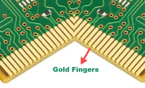
In consumer and prototype electronics, connectors and sliding contacts experience mechanical stress that quickly degrades bare copper or softer finishes. Hard gold addresses this by combining hardness from alloying elements such as cobalt or nickel with gold’s inherent corrosion resistance. Industry standards define minimum plating thicknesses to ensure performance across different classes of use. Proper application extends the service life of edge fingers on expansion cards or repeated-connect devices without significantly increasing resistance. Hobbyists benefit because selective plating allows targeted enhancement of only the contact areas, preserving solderability elsewhere on the board.
Technical Principles of the Electroplating Process
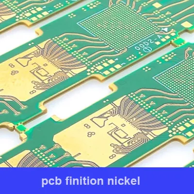
Electroplating deposits metal ions from an electrolyte solution onto a conductive substrate through the application of direct current. For hard gold, the sequence typically begins with thorough cleaning of the copper surface to remove oxides and contaminants. A nickel strike or full nickel layer follows to create a barrier, after which the gold solution plates the final hard deposit. Current density, bath temperature, and plating time directly influence deposit thickness and uniformity. Standards such as IPC-6012E outline qualification requirements for rigid boards including plated finishes, emphasizing adhesion and thickness consistency. The resulting gold layer ranges from flash thicknesses for light-duty contacts to heavier deposits for high-cycle applications, always over the nickel underplate to avoid porosity issues.
Practical Steps for Home Implementation
Begin by masking all areas not intended for plating using tape or resist to confine deposition to the desired contacts. Clean the exposed copper thoroughly with appropriate degreasers and micro-etch solutions, followed by rinsing. Set up a small plating tank or use brush-plating techniques for localized work. First apply the nickel layer using a compatible nickel solution and controlled current, ensuring complete coverage. Rinse again before transferring to the hard gold electrolyte. Maintain recommended voltage and monitor plating duration to reach target thickness without excessive buildup. Post-plating rinsing and drying prevent residue that could affect performance. Always work in a well-ventilated area and follow chemical handling guidelines to minimize risks associated with plating solutions.
Best Practices and Safety Considerations
Consistent agitation or solution movement helps achieve even plating distribution. Test small areas first to calibrate parameters for your specific setup and solution chemistry. Adhere to thickness guidelines referenced in standards like IPC-4556 for plated finishes to balance durability with material usage. Wear appropriate personal protective equipment including gloves and eye protection when handling electrolytes. Dispose of spent solutions according to local regulations rather than pouring them down drains. These steps ensure both functional plating results and responsible hobbyist practices.
Troubleshooting Common Issues in Hobbyist Settings
Uneven plating often stems from inadequate surface preparation or inconsistent current distribution; improve masking and ensure good electrical contact to the workpiece. Poor adhesion usually traces back to residual contaminants or skipped nickel barrier steps. If deposits appear dull or porous, review bath temperature and current density settings. Selective plating demands precise masking to avoid stray deposition on solderable pads, which could impair joint reliability later.
Conclusion
Hard gold plating offers hobbyists a practical method to enhance contact durability on home electronics projects. By following a structured nickel-then-gold sequence and respecting basic process controls, reliable results become achievable with modest equipment. Attention to preparation, safety, and standard-aligned thicknesses supports consistent performance across prototypes and finished assemblies.
FAQs
Q1: What makes hard gold plating suitable for DIY electronics projects?
A1: Hard gold plating delivers wear-resistant contacts through an electrolytic process that hobbyists can replicate at home using controlled solutions and power supplies. It excels on edge connectors and mating surfaces where repeated use would otherwise degrade softer finishes, providing long-term conductivity without complex factory equipment.
Q2: How thick should the gold layer be for home-plated PCB fingers?
A2: Typical hobbyist applications target 30 to 50 microinches of hard gold over a nickel underplate, consistent with guidance in standards such as IPC-6012E for reliable contact performance. Thinner flash layers suffice for low-wear uses while heavier deposits suit higher cycle counts.
Q3: Do I need to plate nickel before applying gold in a DIY setup?
A3: Yes, a nickel barrier layer is essential to prevent copper diffusion into the gold and to promote adhesion. Skipping this step commonly leads to poor durability and increased contact resistance over time.
Q4: What safety precautions apply when performing DIY hard gold plating?
A4: Work in a ventilated space, use chemical-resistant gloves and eye protection, and handle all plating solutions according to manufacturer guidelines. Proper waste disposal prevents environmental contamination from spent electrolytes.
References
IPC-6012E — Qualification and Performance Specification for Rigid Printed Boards. IPC, 2017
IPC-4556 — Specification for Electroless Nickel/Electroless Palladium/Immersion Gold (ENEPIG) Plating for Printed Circuit Boards. IPC, 2013





