 ALLPCB


What Is Dielectric Thickness and Voltage Breakdown
Dielectric thickness refers to the distance between conductive layers in a printed circuit board that provides electrical isolation. Voltage breakdown happens when the insulating material can no longer withstand the applied electric field, leading to a sudden conductive path. Dielectric strength measures the maximum electric field a material can endure before breakdown. In PCB insulation, these factors determine whether a board meets operational requirements.
High voltage PCB design requires careful management of dielectric thickness to avoid premature failure. Creepage and clearance distances complement thickness considerations by addressing surface and through-air paths. Industry standards guide minimum requirements for these parameters. Understanding these relationships helps engineers create robust layouts.
Why Dielectric Thickness Matters in PCB Reliability
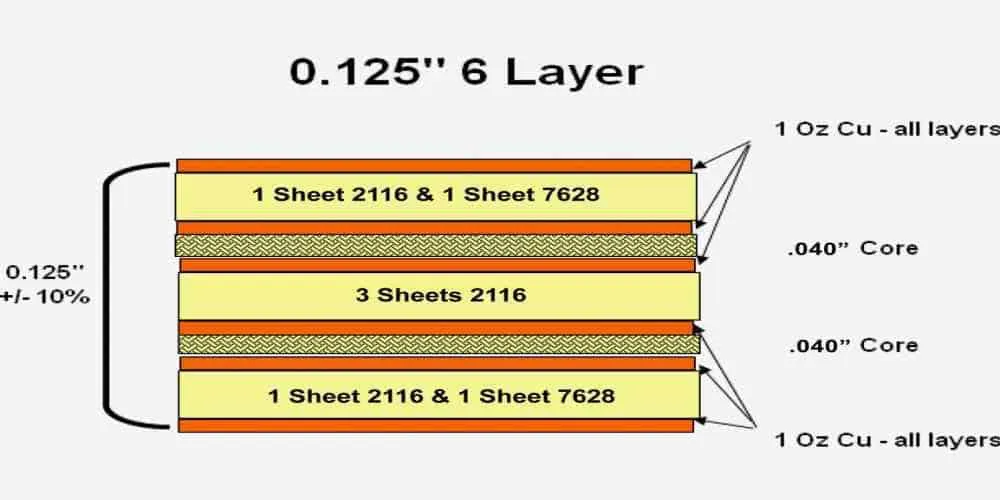
Insufficient dielectric thickness reduces the margin against voltage breakdown, increasing the risk of short circuits or arcing. In multilayer boards, variations in thickness can create weak points that fail under transient voltages. Consistent thickness across production lots supports predictable performance. This consistency proves especially important in applications involving elevated voltages or harsh environments.
PCB insulation integrity also depends on how dielectric thickness interacts with operating temperature and humidity. Thicker layers generally provide higher breakdown resistance, yet excessive thickness may affect signal integrity or thermal management. Engineers balance these trade-offs during the design phase. Reliable insulation contributes to overall system safety and longevity.
Technical Principles of Voltage Breakdown
Voltage breakdown in dielectrics follows principles governed by the electric field strength exceeding the material's dielectric strength. The field intensifies as voltage rises or thickness decreases, concentrating stress at defects or interfaces. Partial discharges may precede full breakdown, gradually degrading the insulation. These mechanisms explain why thickness control remains critical in high voltage PCB design.
Creepage and clearance distances address surface tracking and air ionization paths that can bypass bulk dielectric thickness. Surface contamination or moisture reduces effective creepage performance. Material selection influences both bulk breakdown and surface behavior. Structured analysis of field distribution helps identify potential failure locations before fabrication.
Best Practices for High Voltage PCB Design
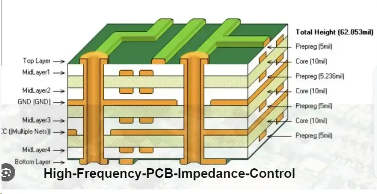
Engineers begin by selecting base materials with appropriate dielectric properties for the target voltage range. Layer stackup planning ensures adequate thickness between high-voltage nets and adjacent conductors. Simulation tools model electric field distribution to verify margins. Design rules incorporate both thickness requirements and creepage and clearance calculations.
During layout, high-voltage traces receive additional spacing and shielding where needed. Manufacturing processes must maintain thickness tolerances to preserve design intent. Quality control checks verify dielectric integrity through appropriate testing methods. Documentation of these steps supports traceability and future revisions.
Practical Considerations for Creepage and Clearance
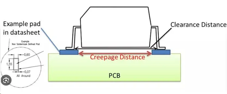
Creepage distances account for surface paths along the board, while clearance addresses the shortest air gap between conductors. Both increase with higher voltages and harsher pollution levels. Designers apply coordinated insulation principles to determine minimum values. These distances work together with dielectric thickness to provide comprehensive insulation.
Environmental factors such as altitude and humidity influence required creepage and clearance. Boards operating in contaminated atmospheres need greater surface distances. Material coatings can enhance surface performance when properly applied. Regular review of these parameters during design iterations improves overall PCB insulation effectiveness.

Conclusion
Dielectric thickness and voltage breakdown represent fundamental considerations in achieving reliable PCB insulation. Structured attention to material selection, layer configuration, and creepage and clearance distances supports robust high voltage PCB design. Consistent application of engineering principles reduces failure risks. These practices ultimately contribute to dependable electronic systems.
FAQs
Q1: What role does dielectric strength play in high voltage PCB design?
A1: Dielectric strength defines the maximum electric field an insulating material can withstand before voltage breakdown occurs. In high voltage PCB design, engineers select materials and thicknesses that provide adequate margins above expected operating voltages. This approach ensures PCB insulation remains effective under normal and transient conditions. Proper consideration of dielectric strength supports overall board reliability.
Q2: How do creepage and clearance affect PCB insulation performance?
A2: Creepage and clearance establish minimum distances along surfaces and through air to prevent arcing or tracking. These parameters complement dielectric thickness by addressing paths outside the bulk material. In high voltage PCB design, coordinated values based on voltage and environment maintain insulation integrity. Adequate creepage and clearance reduce the likelihood of surface-related failures.
Q3: Why is dielectric thickness critical for preventing voltage breakdown?
A3: Dielectric thickness determines the distance over which the electric field acts within the insulating material. Thinner sections experience higher field stress at a given voltage, lowering the threshold for voltage breakdown. Consistent thickness across the board supports uniform PCB insulation behavior. Engineers verify thickness during design and manufacturing to preserve performance margins.
Q4: What standards guide dielectric thickness requirements in PCBs?
A4: Standards such as IPC-6012E provide qualification criteria for rigid printed boards, including aspects relevant to insulation. IEC standards address insulation coordination for equipment operating at various voltages. These documents help engineers establish appropriate dielectric thickness and related parameters. Reference to established standards promotes consistent and reliable outcomes.
References
IPC-6012E — Qualification and Performance Specification for Rigid Printed Boards. IPC, 2017
IEC 60664-1 — Insulation coordination for equipment within low-voltage systems — Part 1: Principles, requirements and tests. IEC, 2007
ASTM D149 — Standard Test Method for Dielectric Breakdown Voltage and Dielectric Strength of Solid Electrical Insulating Materials at Commercial Power Frequencies. ASTM International, 2020


