 ALLPCB


Designing Robotics PCBs: Balancing Performance and Miniaturization
Robotics systems demand printed circuit boards that deliver high computational power, precise sensor interfacing, and reliable motor control within extremely limited physical envelopes. Engineers face the dual challenge of maintaining signal integrity and thermal performance while shrinking board dimensions to fit articulated arms, mobile bases, or compact end-effectors. High-density PCB for robotics enables the integration of microcontrollers, power management integrated circuits, and communication modules without compromising functionality. Compact PCB design techniques allow robotics platforms to achieve greater mobility and lower inertia, which directly improves dynamic response and energy efficiency. Small form factor PCB solutions have become essential as robotics applications expand into collaborative manufacturing, medical assistance, and autonomous logistics.
Why Miniaturization Matters in Robotics PCB Design
The physical constraints of robotic mechanisms make board size and weight critical design parameters. A reduction in PCB area and mass lowers the overall payload on joints and actuators, which extends operational life and reduces power consumption. Miniaturized robotics circuits also permit tighter integration of sensing, processing, and actuation functions on a single substrate, shortening signal paths and reducing electromagnetic interference. Industry requirements for higher payload-to-weight ratios and faster cycle times continue to drive demand for these compact solutions. Engineers must therefore evaluate every layer stack-up decision against both electrical performance targets and mechanical envelope limits.
Technical Principles of High-Density and Compact PCB Design
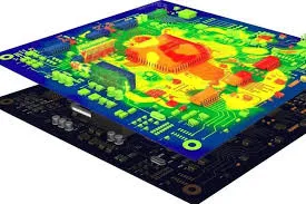
High-density interconnect technology relies on finer line widths, smaller vias, and sequential lamination processes to achieve greater routing density. These features allow designers to route hundreds of signals within a footprint that would otherwise require multiple larger boards. Thermal management becomes more challenging as component density increases, because heat generated by processors and power devices must dissipate through reduced copper areas and thinner dielectric layers. Signal integrity analysis must account for shorter trace lengths that can still exhibit impedance discontinuities if via stubs or layer transitions are not optimized. Mechanical considerations include controlling board warpage during reflow and ensuring adequate stiffness for vibration environments typical in robotic motion.
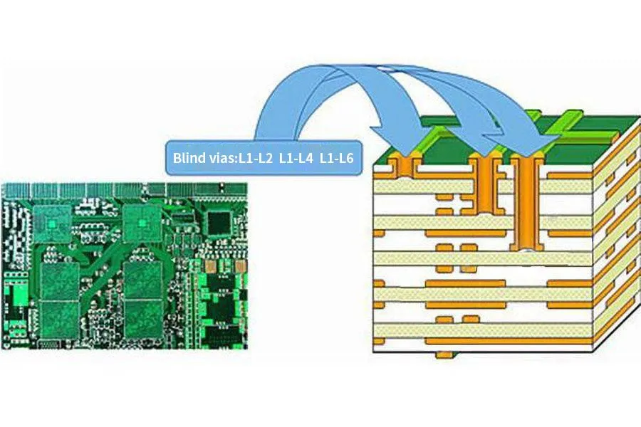
Component placement strategies emphasize clustering high-speed devices near their associated power and ground planes while maintaining adequate spacing for thermal relief. Flexible or rigid-flex constructions further reduce overall volume by allowing boards to conform to curved surfaces or fold into three-dimensional assemblies. Material selection focuses on laminates with appropriate glass transition temperatures and coefficients of thermal expansion to maintain reliability under repeated thermal cycling. Design rules must incorporate minimum annular ring requirements and copper balance guidelines to prevent manufacturing defects that become more probable at reduced feature sizes.
Practical Solutions and Best Practices
Designers begin by establishing clear electrical and mechanical specifications that quantify maximum board dimensions, allowable warpage, and target operating temperatures. Early-stage simulation of power distribution networks and high-speed signal paths identifies potential bottlenecks before layout begins. Layer stack-up planning balances the need for additional signal layers against the desire to keep overall thickness low for weight savings. Via-in-pad technology and filled microvias help reclaim routing real estate while maintaining planarity for fine-pitch component attachment.
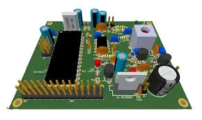
Thermal vias and strategic copper pours under heat-generating components improve heat spreading without adding significant board area. Careful attention to ground plane continuity and stitching vias maintains return paths for high-frequency signals even in densely populated regions. Design for manufacturability reviews incorporate checks for minimum feature sizes, aspect ratios of vias, and solder mask clearances that align with accepted industry practices. Iterative prototyping with representative mechanical fixtures validates both electrical performance and physical fit before committing to production volumes.
Quality and Reliability Considerations
Reliability in miniaturized robotics PCBs depends on adherence to established qualification procedures that verify both electrical and mechanical integrity. Controlled impedance testing confirms that transmission lines meet target values despite the reduced geometries. Accelerated life testing under combined temperature, humidity, and vibration stresses reveals weaknesses that may not appear during initial functional checks. Documentation of material properties and process parameters supports traceability required for safety-critical robotic applications.
Conclusion
Balancing performance and miniaturization in robotics PCB design requires systematic attention to electrical, thermal, and mechanical domains from the earliest concept stage. High-density techniques, advanced stack-ups, and rigorous simulation enable engineers to meet aggressive size targets without sacrificing functionality or reliability. Continued refinement of placement strategies and material choices will support the next generation of more capable and compact robotic systems.
FAQs
Q1: How does high-density PCB for robotics improve overall system performance?
A1: High-density PCB for robotics allows more components and shorter interconnects within a smaller footprint, which reduces signal propagation delays and electromagnetic interference while lowering weight and inertia. These improvements enhance responsiveness and energy efficiency in robotic motion.
Q2: What are the main challenges in achieving compact PCB design for robotic applications?
A2: Compact PCB design must address increased thermal density, tighter routing constraints, and the need to maintain mechanical stability under vibration. Engineers balance these factors through careful stack-up planning and component placement that respects both electrical and physical limits.
Q3: Why is small form factor PCB important for miniaturized robotics circuits?
A3: Small form factor PCB enables tighter integration of control, sensing, and power functions directly on moving robot segments. This integration reduces cabling complexity, improves reliability, and allows robots to operate in confined spaces.
Q4: What role do industry standards play in ensuring reliability of miniaturized robotics circuits?
A4: Standards such as those from IPC and JEDEC provide consistent criteria for board qualification, acceptability, and moisture sensitivity that help ensure long-term performance under demanding robotic operating conditions.
References
IPC-6012E — Qualification and Performance Specification for Rigid Printed Boards. IPC, 2017
IPC-A-600K — Acceptability of Printed Boards. IPC, 2020
JEDEC J-STD-020E — Moisture/Reflow Sensitivity Classification. JEDEC, 2014
ISO 9001:2015 — Quality Management Systems. ISO, 2015





