 ALLPCB


Introduction
The electronics industry continues to evolve under increasing regulatory and market pressures to reduce environmental impact. Sustainable PCB laminates represent a significant advancement in this direction. These materials incorporate alternative resins, reinforcements, and formulations that lower the use of hazardous substances while maintaining necessary electrical and mechanical properties. Engineers and designers must evaluate these options carefully to balance performance requirements with sustainability goals. Adoption of such laminates supports broader efforts in sustainable electronics design across multiple sectors.
What Are Sustainable PCB Laminates and Why They Matter
Sustainable PCB laminates differ from conventional materials primarily through their composition and end-of-life characteristics. They often feature halogen-free flame retardants, bio-based or recycled resin systems, and reinforcements derived from natural fibers or recycled sources. These changes address concerns over toxic emissions during manufacturing and disposal. The shift matters because electronic waste volumes continue to grow, and material choices at the design stage directly influence recyclability and regulatory compliance. Procurement teams and design engineers increasingly prioritize these laminates to meet corporate environmental targets without sacrificing board reliability.
Industry standards guide the qualification of these materials to ensure they perform equivalently to traditional options in demanding applications. Factory processes must adapt to handle variations in thermal expansion or moisture absorption that can occur with new formulations. This relevance extends to high-volume production environments where consistency remains critical.
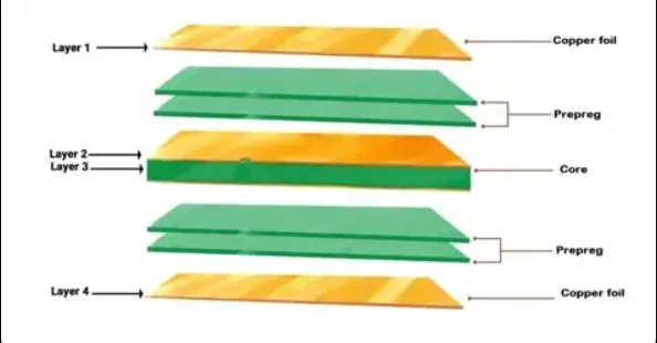
Technical Principles of Sustainable Laminate Performance
Sustainable laminates achieve reduced environmental impact through targeted modifications to the resin matrix and reinforcement layers. Halogen-free systems replace bromine or chlorine compounds with phosphorus-based or mineral fillers that maintain flame retardancy. Bio-derived epoxies or modified polyimides can lower the carbon footprint associated with raw material extraction and processing. These alterations influence key properties such as glass transition temperature, dielectric constant, and coefficient of thermal expansion.
Engineers evaluate these parameters during material selection to prevent issues like delamination or signal integrity degradation. Manufacturing facilities monitor cure cycles and lamination pressures more closely when processing alternative materials. Performance testing follows established protocols to verify that boards withstand assembly temperatures and operational stresses. The mechanisms involved center on molecular structure adjustments that preserve insulation resistance and mechanical strength while eliminating persistent environmental pollutants.
Related Reading: Sustainable Flexible PCBs: Eco-Friendly Materials for Wearable Electronics
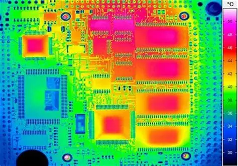
Practical Solutions and Best Practices for Implementation
Design teams begin by reviewing laminate datasheets against application-specific requirements for frequency, power, and environmental exposure. Selection criteria include compatibility with lead-free soldering processes and long-term reliability under humidity. Collaboration between design and manufacturing ensures that stack-up configurations account for any differences in flow characteristics during lamination.
Related Reading: Sustainable PCB Layout: Choosing Lead Free Components and Materials
Best practices include conducting thorough qualification testing on prototype boards before full production. This involves thermal cycling, interconnect stress testing, and surface insulation resistance measurements. Supply chain teams verify that chosen materials carry appropriate certifications for restricted substance compliance. Documentation of material properties supports traceability and future audits. When transitioning to sustainable options, iterative design reviews help identify and mitigate potential warpage or via reliability concerns early.
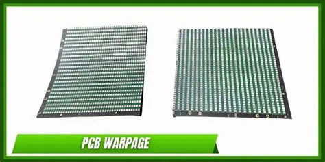
Additional steps involve updating design rules for via fill materials and copper foil adhesion when using new resin systems. Engineers document these adjustments to maintain consistency across product revisions. Regular process capability studies in the factory confirm that yield rates remain stable after material changes.
Conclusion
Sustainable PCB laminates offer a viable pathway for the electronics sector to advance environmental objectives while preserving functional performance. Through careful material evaluation and adherence to qualification processes, engineers can integrate these options effectively. Continued refinement of formulations and manufacturing techniques will further expand their applicability. The result supports more responsible product lifecycles from design through disposal.
FAQs
Q1: How do sustainable materials support eco friendly PCB design guide objectives?
A1: Sustainable laminates enable designers to meet environmental targets by reducing hazardous content and improving end-of-life options. Selection involves matching electrical and thermal specifications to application needs while confirming compliance with relevant performance standards. This approach integrates into existing design workflows without requiring complete process overhauls.
Q2: What defines the future of PCB materials in electronics manufacturing?
A2: The future centers on formulations that deliver equivalent reliability with lower environmental impact. Key developments include enhanced bio-based resins and improved recycling compatibility. Engineers assess these materials through standardized testing to ensure they withstand assembly and operational conditions across diverse applications.
Q3: Which innovative PCB laminates best suit high-reliability applications?
A3: Innovative options combine halogen-free chemistry with optimized reinforcements for stable performance under thermal and mechanical stress. Evaluation focuses on properties such as moisture resistance and dimensional stability. Manufacturers validate these laminates through qualification sequences aligned with industry specifications.
Q4: How can teams incorporate sustainable materials for electronics in new projects?
A4: Teams start with a review of required board characteristics and then identify candidate laminates that satisfy both performance and environmental criteria. Prototyping and testing confirm suitability before scaling. Documentation of decisions supports ongoing compliance and process optimization efforts.
References
IPC-4101D — Specification for Base Materials for Rigid and Multilayer Printed Boards. IPC, 2017
ISO 14001:2015 — Environmental Management Systems. ISO, 2015
IPC-6012E — Qualification and Performance Specification for Rigid Printed Boards. IPC, 2017





