 ALLPCB


Introduction
Depaneling represents a critical final step in PCB manufacturing, where individual boards are separated from production panels after assembly. This process must balance efficiency with precision to avoid introducing defects that compromise long-term reliability. As PCB designs evolve toward higher densities with fine-pitch components and multilayer stacks, the risks associated with mechanical forces during separation become more pronounced. Engineers face the challenge of selecting depaneling machines and techniques that preserve board flatness and component functionality. Effective strategies focus on PCB stress reduction methods to prevent issues like microcracking or delamination. Ultimately, mastering low-stress depaneling techniques ensures higher yields and robust performance in end applications.
Understanding PCB Depaneling and Its Importance
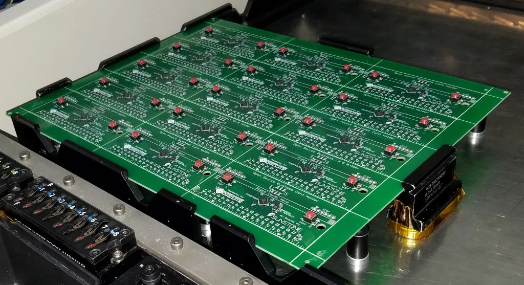
PCB depaneling involves severing the connections, such as V-scores, perforations, or tabs, that hold multiple boards together in a panel format. Panels optimize manufacturing throughput during fabrication and assembly, but separation requires careful control to maintain structural integrity. Poor depaneling can lead to component damage during depaneling, including solder joint failures in BGAs or ceramic capacitors, which manifest as field failures months later. Industry demands for reliability, especially in automotive and aerospace sectors, underscore the need for processes aligned with quality benchmarks like IPC-6012 for rigid board specifications. By prioritizing component integrity, manufacturers reduce rework and enhance overall product lifespan. This stage directly influences the acceptability criteria outlined in standards such as IPC-A-600.
The relevance extends to factory operations where depaneling bottlenecks can slow production lines. High-volume runs benefit from automated machines that handle varied panel layouts without compromising quality. Engineers must consider board thickness, material type like FR-4, and component proximity to edges when planning. Neglecting these factors amplifies risks from vibrational or flexural loads. Proactive design for depaneling integrates seamlessly with upstream processes, minimizing downstream quality control efforts.
Mechanisms of Stress Generation in Depaneling
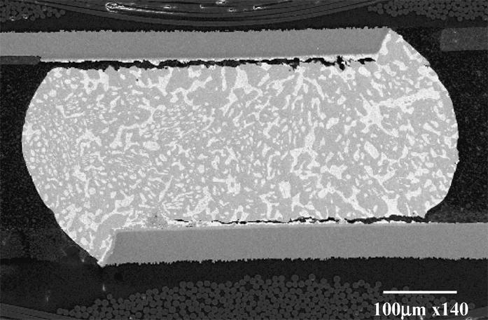
Stress in PCBs arises primarily from mechanical forces applied during separation, including bending moments, shear, and localized pressures. In V-groove methods, the board flexes until the score line fractures, creating peak tensile and compressive strains perpendicular to the cut direction. These forces propagate through the laminate, potentially causing interlayer delamination or via barrel cracks. Router-based systems introduce vibrational energy from spindle rotation, though proper fixturing dissipates much of it. Laser ablation, by contrast, vaporizes material without physical contact, eliminating bulk deformation. Understanding strain distribution helps predict vulnerable areas near plated through-holes or surface-mount devices.
Component damage during depaneling often stems from dynamic loading rates that exceed material yield points. Fine-pitch QFNs or wire-bonded chips experience shear at terminations if unsupported. Multilayer boards with thin cores amplify warpage under uneven stress fields. Thermal residues from prior reflow can precondition the assembly, making it more susceptible to brittle failure. Factory-driven insights emphasize monitoring strain limits as per IPC/JEDEC-9704 guidelines, which recommend gage placement to capture peak responses. This data informs process adjustments for consistent outcomes.
Environmental factors like humidity can exacerbate issues by softening adhesives, but mechanical dominance prevails. Vibration from inline conveyors transmits to the panel, compounding local effects. Edge quality post-depaneling affects conformal coating adhesion, indirectly impacting durability. Engineers model these interactions using finite element analysis during design validation.
Common Causes of PCB Stress and Component Damage
Manual breaking along perforations delivers the highest shock loads, often resulting in microcracks invisible to optical inspection. Operators apply inconsistent force, leading to over-flexure that damages hidden solder fillets. V-scoring with shearing blades reduces this somewhat but still generates localized heating and chipping. Punching employs dies for high-speed separation, yet the impulsive force risks board bounce and component displacement. These methods prove unsuitable for densely populated panels with tall components.
Routing mills tabs sequentially, but dull bits or excessive feed rates elevate torque and chatter. Dust accumulation clogs fixtures, altering support dynamics and increasing deflection. Sawing straight lines suits thick substrates but vibrates sensitive optics nearby. Proximity of components to cut paths dictates failure modes; those parallel to the direction fare better than perpendicular ones. Poor panel design, like inadequate tab spacing, concentrates loads. Component damage during depaneling manifests as intermittent opens or parametric drifts in analog circuits.
Handling post-separation introduces secondary risks if boards lack edge support. Warped panels from baking unevenly distribute forces. Fixture misalignment during machine setup amplifies all vectors.
Low-Stress Depaneling Techniques Explained
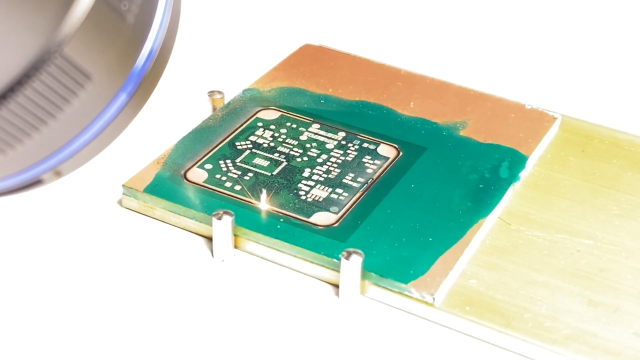
Laser depaneling stands out for its non-contact nature, using focused UV beams to ablate material layer by layer. This technique produces negligible vibration, ideal for high-density interconnect boards or flex-rigid hybrids. Kerf widths remain minimal, maximizing panel utilization without tabs. It accommodates irregular contours where mechanical tools falter. Setup involves CAD import for path optimization, ensuring clean edges free of burrs.
Router depaneling with high-speed spindles offers versatility for tab-routed panels. Vacuum fixturing secures the array, while vision alignment prevents offsets. Low-stress variants employ sharp, fine-flute bits and controlled Z-axis plunges. This method suits medium volumes with complex outlines. Dust extraction maintains cleanliness, preventing abrasive wear on optics.
V-groove rolling blades provide a cost-effective option for straight separations. Circular cutters follow the score progressively, distributing force better than snapping. Automated versions with linear guides enhance repeatability. Waterjet streams erode material coldly, avoiding heat zones, though drying adds steps.
Punching works for simple geometries in high volumes, with dies conforming to contours. Stress minimizes through matched upper-lower tooling and progressive staging.
Best Practices for PCB Stress Reduction Methods
Integrate depaneling planning into PCB layout, specifying clearances like ample spacing from edges for mechanical methods. Orient sensitive components parallel to anticipated cut lines to lower perpendicular strains. Employ full-panel fixturing with distributed supports under populated areas. Validate setups using strain gages per IPC/JEDEC-9704 protocols to benchmark against thresholds.
Optimize machine parameters: reduce spindle speeds for routers, align blade angles precisely for V-scores. Implement inline monitoring for bit wear or laser focus drift. Post-process inspections include dye penetrant for cracks and electrical continuity tests. Panel design favors mouse bites over full tabs for gradual release.
Train operators on gentle handling and ESD protocols during transfer. Simulate processes virtually to predict hotspots. Collaborate with fabrication partners on scoring depth uniformity.
Troubleshooting Depaneling-Induced Issues
Warpage post-depaneling signals asymmetric stress; counter with symmetric tab placement or laser for uniform relief. Solder bead cracks indicate excessive flex; switch to routing or verify component standoffs. Dust contamination on fiducials disrupts vision systems; enhance extraction and air blasts. Inconsistent edges from blade wander require sharpening schedules and runout checks.
If delamination appears, review laminate quality against IPC-6012 criteria. Parametric shifts in passives suggest vibration overload; add damping materials to fixtures. Field returns tracing to depaneling prompt root-cause strain mapping.
Conclusion
Minimizing PCB stress during depaneling safeguards component integrity through method selection, design foresight, and rigorous process control. Low-stress techniques like laser and optimized routing deliver superior outcomes for modern assemblies. Adhering to standards ensures compliance and reliability. Factories gain efficiency by reducing defects and rework. Engineers achieve optimal results by balancing cost, volume, and quality demands. Prioritizing these PCB stress reduction methods elevates manufacturing excellence.
FAQs
Q1: What are effective PCB stress reduction methods for high-density boards?
A1: Low-stress depaneling techniques such as laser ablation and precision routing minimize mechanical forces. Fixturing supports the panel fully, while component orientation parallel to cuts reduces perpendicular strain. Strain gage testing per IPC/JEDEC-9704 verifies limits during trials. Design clearances exceed 0.5mm for routers, enhancing integrity. These approaches suit fine-pitch assemblies in demanding applications.
Q2: How does component damage during depaneling occur and how to prevent it?
A2: Damage arises from flexural shock cracking solder joints or dislodging terminations, especially in BGAs. Manual snapping or punching amplifies risks through impulse loads. Prevention involves non-contact lasers or controlled routers with vibration damping. Maintain edge clearances and validate via electrical tests post-process. Proper fixturing distributes forces evenly across the panel.
Q3: Which low-stress depaneling techniques work best for complex PCB shapes?
A3: Router and laser methods excel for curves and irregular outlines, avoiding V-score limitations. Routers mill tabs precisely with CNC paths, while lasers follow any contour contact-free. Both generate low vibration, preserving nearby components. Factory validation includes first-article inspections for edge quality. These techniques align with high-reliability needs.
Q4: Why monitor strain during depaneling per industry standards?
A4: Standards like IPC/JEDEC-9704 guide gage placement to quantify peak strains, preventing latent failures. Exceeding thresholds risks microcracks propagating under thermal cycling. Monitoring enables parameter tweaks for consistent low-stress outcomes. It supports qualification for IPC Class 3 products. This factory-driven practice boosts yield and traceability.
References
IPC/JEDEC-9704 - Printed Wiring Board Strain Gage Test Guideline. IPC/JEDEC, 2005
IPC-6012E - Qualification and Performance Specification for Rigid Printed Boards. IPC, 2017
IPC-A-600K - Acceptability of Printed Boards. IPC, 2020


