 ALLPCB


Introduction
Manual PCB depaneling offers electronic hobbyists a straightforward way to separate individual circuit boards from a production panel without investing in expensive machinery. This hands-on approach appeals to those prototyping small batches or experimenting in home workshops, where speed and simplicity often trump high-volume precision. However, hand breaking PCBs carries inherent risks, such as unintended stress that could compromise board integrity over time. Understanding when this method suits your project helps balance convenience with reliability. For hobbyists tackling custom designs or repairs, knowing the limits of manual techniques ensures projects succeed without costly rework. This article explores the conditions under which hand depaneling proves acceptable, drawing on established practices to guide safe execution.
What Is Manual PCB Depaneling and Why It Matters
Manual PCB depaneling involves physically separating individual printed circuit boards from a larger panel using hand-applied force, typically along predefined weak points like V-scores or perforations. Common techniques include snapping along V-grooves, where the panel features angled cuts on both sides, or clipping perforated tabs known as mouse bites. Hobbyists favor this for its zero-equipment cost and immediate results, ideal for one-off prototypes or educational builds. Yet, it matters because improper execution introduces mechanical stress that may lead to hidden defects, affecting long-term performance in powered circuits. In contrast to automated routing or laser methods, hand depaneling demands careful control to preserve trace integrity and component alignment. For electronic enthusiasts, mastering these basics elevates project quality while avoiding common pitfalls.
The relevance grows in hobbyist settings, where panels arrive from fabricators optimized for simple separation. V-scored panels, for instance, allow clean breaks if designed correctly, minimizing waste. However, post-assembly boards with soldered components heighten vulnerability, as bending forces propagate unevenly. Recognizing these dynamics empowers hobbyists to choose wisely between hand methods and professional services. Ultimately, manual approaches shine in low-stakes scenarios but falter under demanding reliability needs.
Technical Principles of Hand Depaneling PCBs
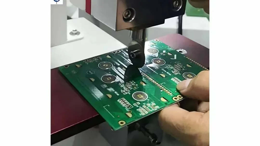
Hand depaneling relies on engineered break lines in the panel design, such as V-scoring, which creates partial grooves typically aligned to facilitate snapping without full-thickness cuts. These grooves reduce the material bridge, concentrating force along a predictable path during manual separation. The process induces bending stress across the board, potentially straining copper traces, vias, and laminate layers if the panel lacks symmetry or sufficient support. IPC-2221 outlines design guidelines for such features, emphasizing uniform scoring depth and board thickness compatibility to mitigate risks. Uneven pressure during the break can cause localized microcracking, especially near edges or mounted components. Understanding these mechanics helps hobbyists anticipate failure modes and adapt their technique accordingly.
Material properties play a key role, as standard FR4 laminates exhibit varying flexibility based on thickness and glass transition temperature. Thinner boards bend more readily, distributing stress evenly, while thicker ones resist, amplifying peak loads at score lines. Perforations or tabs serve as alternative weak points, requiring sequential clipping to avoid panel warp. The goal remains controlled fracture, preserving edge quality for subsequent soldering or enclosure fitting. Hobbyists benefit from visualizing stress flow, akin to breaking a chocolate bar along scores, to achieve repeatable results.
When Is Hand Depaneling Acceptable?
Hand depaneling becomes acceptable primarily for prototype panels with simple rectangular layouts and V-scoring or perforation designs intended for manual separation. It suits electronic hobbyists working with low-component-density boards, where sensitive parts like fine-pitch SMDs stay clear of edges. Pre-assembly depaneling proves ideal, as it avoids stressing soldered joints or tall components that could snag during flexing. Panels from fabricators specifying hand-break compatibility signal suitability, often featuring scores to about one-third board thickness on opposing faces. For hobby projects emphasizing quick iteration over longevity, this method delivers without overcomplication.
Avoid it for densely populated assemblies or irregular shapes, where force application proves unpredictable. Post-SMT boards risk component leads cracking under torque, particularly quad flat no-leads packages prone to pad lift-off. Board thickness influences viability; standard hobbyist prototypes tolerate manual methods better than rigid, multi-layer stacks. If the panel includes fiducials or markings for automated tools, hand breaking may misalign features. Assessing these factors upfront determines if manual PCB depaneling aligns with project tolerances.
Production-like reliability demands mechanical alternatives, but hobbyists gain flexibility here. Acceptable scenarios cluster around educational kits, Arduino shields, or sensor boards with generous margins. Always inspect design files for depaneling intent before proceeding.
Best Practices and PCB Depaneling Tools for Safe Execution
Start with proper setup: secure the panel on a soft, flat surface like foam or rubber matting to distribute support and prevent backside scratches during breaking. Wear safety glasses and cut-resistant gloves, as shards from laminate can fly. For V-scored panels, align the score line over a straight edge, such as a workbench lip, and apply gradual, even pressure from one end to propagate the break cleanly. Use manual PCB depaneling tools like shear pliers for tabs or perforations, gripping firmly without twisting to minimize lateral stress. Support both sides of the board equally to avoid bowing, which induces unnecessary strain on inner layers.
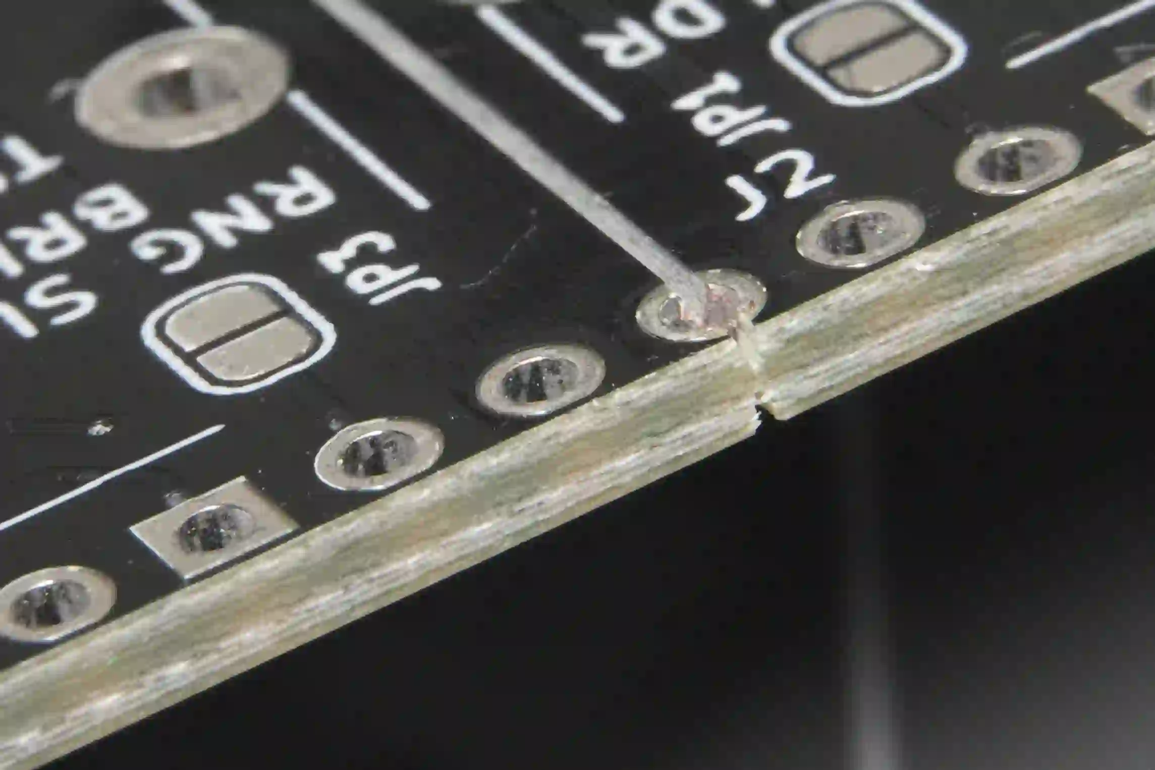
Progress sequentially: depanel one board at a time, starting from outer edges inward to maintain panel stability. Post-break, deburr edges with fine sandpaper or a file, focusing on copper-exposed areas to prevent shorts. Inspect under magnification for cracks, lifted traces, or delamination signs per IPC-A-600 acceptability criteria, rejecting any with visible defects. Store separated boards flat to prevent warpage from residual stresses. These steps form acceptable practices for hand depaneling, prioritizing damage avoidance.
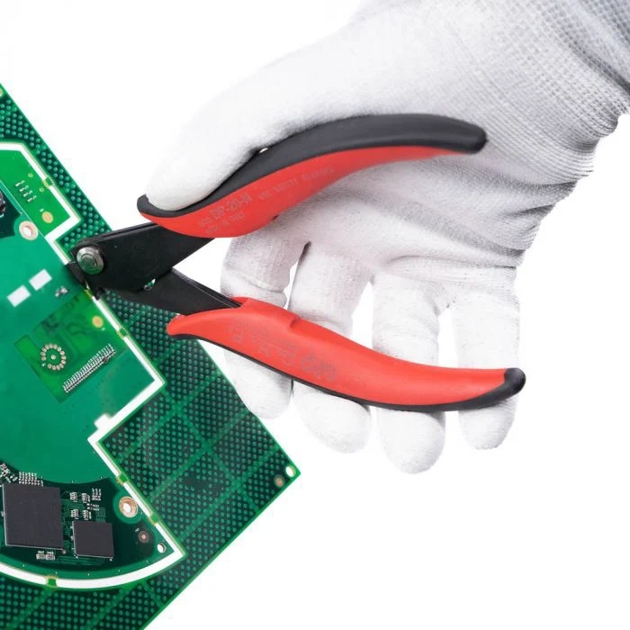
Incorporate fixtures if repeating processes; a simple wooden jig with slots matching score lines enhances precision. Test on scrap panels first to gauge force needed. Clean hands or use anti-static gloves to protect bare copper from oils during handling.
Troubleshooting Common Issues in Hand Depaneling
Uneven breaks often stem from misaligned scoring or excessive force, resulting in jagged edges that snag wires or impede heatsink mounting. Chips along the score line indicate brittle laminate or deep over-scoring; mitigate by slowing the snap and using backing support. Component damage near edges, like SMD tombstoning precursors, arises from vibration transmission; depanel pre-assembly when possible. Warped boards post-separation signal asymmetric stress; flatten under light weight before inspection.
Burrs on copper traces pose short risks; lightly abrade and clean with isopropyl alcohol. If perforations tear irregularly, switch to plier-clipping individual tabs methodically. Persistent microcracks require magnification checks; discard suspect boards for reliability-critical uses. These fixes restore usability while reinforcing technique refinement.
Conclusion
Hand depaneling PCBs proves acceptable for electronic hobbyists in controlled scenarios like V-scored prototypes with low component density and pre-assembly timing. By adhering to design principles from IPC-2221 and edge standards in IPC-A-600, enthusiasts minimize risks while enjoying cost-free separation. Key to success lies in preparation, even force application, and thorough inspection using basic tools. While not suited for high-reliability or complex assemblies, it empowers rapid iteration in home labs. Weigh project needs against potential defects to decide confidently. With practice, manual methods enhance skills without compromising hobby outcomes.
FAQs
Q1: What are the main risks of hand breaking PCBs during manual depaneling?
A1: Hand breaking PCBs risks inducing stress cracks in traces and laminate, especially on thicker boards or near components. Uneven force can cause warpage or lifted pads, compromising solderability. For hobbyists, these issues surface in vibration-prone applications. Mitigate by using V-scored designs and supporting the panel fully. Always inspect edges post-separation to catch defects early.
Q2: When should electronic hobbyists choose manual PCB depaneling tools?
A2: Opt for manual PCB depaneling tools on simple, thin prototype panels with V-scoring or tabs. It's ideal pre-assembly for low-volume projects avoiding machinery costs. Avoid post-SMT if tall components risk damage. Pliers and straight edges suffice for clean results. Confirm panel design supports hand methods first.
Q3: What are acceptable practices for hand depaneling to avoid damage?
A3: Follow acceptable practices for hand depaneling by securing panels on soft surfaces, applying gradual pressure along scores, and wearing safety gear. Deburr and inspect per standards afterward. Limit to symmetric, low-density boards. Sequential tab clipping prevents warp. This ensures reliability for hobbyist builds.
Q4: Can hand depaneling work on assembled PCBs?
A4: Hand depaneling assembled PCBs works cautiously on V-scored panels with minimal edge components, but risks joint stress. Prefer pre-assembly for safety. Use fixtures for stability and inspect for cracks immediately. It's acceptable for prototypes, not production.
References
IPC-2221B - Generic Standard on Printed Board Design. IPC, 2017
IPC-A-600K - Acceptability of Printed Boards. IPC, 2020


