ALLPCB


Introduction
High-density interconnect (HDI) assembly represents a critical step in producing compact, high-performance electronics for applications like smartphones, medical devices, and automotive systems. These boards feature fine-pitch components, microvias, and dense routing, which amplify the risk of defects during surface-mount technology (SMT) processes. Effective HDI assembly defect prevention ensures reliable solder joints, precise component placement, and overall board functionality, minimizing costly rework and field failures. Engineers must prioritize process controls from solder paste printing through final inspection to achieve yield rates above 99 percent in production. This article explores practical strategies tailored for troubleshooting common issues in HDI manufacturing. By implementing these best practices, teams can enhance quality control in HDI environments.
Understanding HDI Assembly and Its Challenges
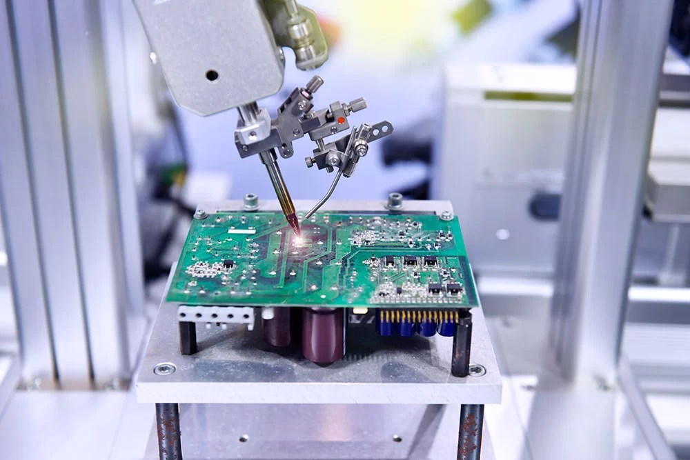
HDI assembly involves placing tiny components onto boards with feature sizes below 100 microns, including blind and buried vias that demand precise alignment. Unlike standard PCBs, HDI boards undergo multiple lamination cycles, resulting in thinner substrates prone to warpage under thermal stress. Common challenges include solder joint defects HDI-specific, such as bridging on 0.3 mm pitch BGAs and voids from uneven reflow heating. Component placement errors arise from high-speed pick-and-place machines struggling with fiducial recognition on dense layouts. These issues directly impact signal integrity and thermal management in end products. Addressing them requires a deep understanding of material interactions and process variables.
Key Causes of Defects in HDI Assembly
Solder joint defects HDI often stem from inadequate solder paste volume control during printing, leading to bridges or insufficient wetting on small pads. Fine particle solder pastes, like Type 4 or 5, can slump if stencil apertures are not optimized, causing shorts between adjacent leads. Reflow profiles with rapid ramps exacerbate head-in-pillow effects, where components float above softened solder without full fusion. Component placement errors occur due to board warpage, where convex bowing lifts edges during vacuum pickup, shifting parts by tens of microns. Vibration in feeders or poor nozzle calibration compounds misalignment, especially for 01005 passives. Via-in-pad designs introduce additional risks like solder wicking into microvias, blocking connections if not plugged properly.
Thermal mismatch between copper-filled vias and laminate contributes to cracks under cyclic loading, a frequent hidden failure mode. Moisture absorption in HDI layers prior to reflow promotes voids and delamination, as steam expands rapidly. Inadequate cleaning leaves flux residues that promote electromigration over time. These root causes highlight the need for proactive HDI assembly defect prevention through design-for-manufacturability (DFM) reviews early in the process. Engineers troubleshooting these must correlate defect patterns with process data logs for targeted fixes.
Best Practices for Solder Paste Application and Stencil Design
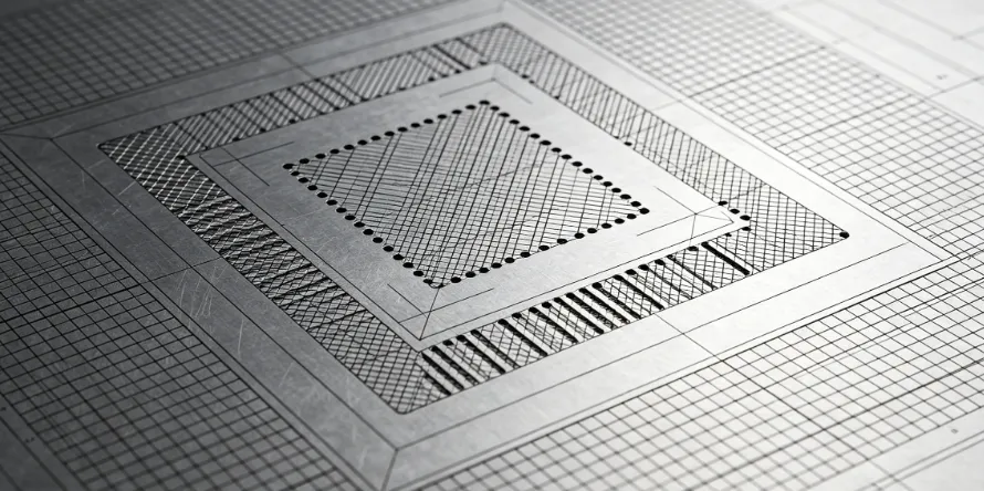
Optimal stencil design forms the foundation of HDI assembly defect prevention by ensuring uniform paste deposition. Use laser-cut stainless steel stencils with thicknesses of 0.1 mm or less for pitches under 0.4 mm, incorporating trapezoidal apertures to reduce paste retention. Implement solder paste inspection (SPI) after printing to verify volume, height, and position within 10 percent tolerances, catching anomalies before placement. Select low-residue, no-clean pastes with metal loads above 88 percent to minimize voids during reflow. Pressure and squeegee speed adjustments, typically 40-60 mm/s, prevent smearing on fine features. Regular stencil cleaning with plasma or ultrasonic methods maintains aperture integrity over high-volume runs.
These steps directly combat solder joint defects HDI by promoting consistent fillet formation and heel wetting. Validation through cross-section analysis confirms paste transfer efficiency above 90 percent.
Precision Component Placement Techniques
Accurate component placement demands fiducials at all board corners and arrays, sized 1 mm with 0.5 mm chrome contrast for machine vision reliability. High-speed placers with 020 micron resolution and downward-looking cameras minimize errors on warped HDI substrates. Employ split-vision systems to detect offsets in real-time, rejecting boards exceeding 25 micron shifts. Vacuum nozzles tailored to component sizes, combined with soft-landing parameters, prevent tombstoning on asymmetric pads. Preheating boards to 100-120 degrees Celsius stabilizes dimensions during transfer. Post-placement automated optical inspection (AOI) verifies alignment against Gerber data, flagging polarity inversions or absences early.
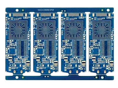
Integrating these practices reduces component placement errors by optimizing machine parameters and substrate handling.
Optimizing Reflow Soldering for Reliable Joints
Reflow profile development is crucial for HDI, starting with a linear ramp to 150 degrees Celsius soak for flux activation, followed by a 2-3 degrees per second peak to 245-260 degrees Celsius. Nitrogen atmospheres at 1000 ppm oxygen limit oxidation on small pads, enhancing wetting. Board supports or mesh conveyors counteract warpage, maintaining planarity within 0.75 percent. Simulate profiles using thermocouples on test coupons to match thermal mass variations from stacked dielectrics. Cooling rates below 4 degrees per second prevent brittle intermetallics. Adhering to J-STD-001 guidelines ensures voiding below 25 percent in BGA balls.
These controls prevent solder joint defects HDI like opens from dewetting or cracks from overstress.
Advanced HDI PCB Inspection and Quality Control
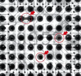
HDI PCB inspection begins with pre-reflow SPI and post-placement AOI, progressing to 3D AOI for height profiling of joints. X-ray systems detect subsurface voids, bridging under BGAs, and via fill in filled microvias. IPC-A-610 criteria classify defects by class, with Class 3 demanding zero visible bridges and full heel fillets. Functional testing via flying probes verifies continuity on dense nets. Traceability software logs all data for root-cause analysis. Implementing statistical process control (SPC) monitors CpK values above 1.33 for critical parameters.
Quality control in HDI integrates these layers to achieve defect rates under 100 DPMO.
Troubleshooting Common HDI Assembly Issues
When solder bridging appears, check stencil release and reduce aperture area by 10-15 percent. Tombstoning signals uneven paste or ramp rates; balance volumes and slow preheat. Warpage exceeding 1 mm calls for symmetric stackups and fixture supports. Voids over 30 percent volume prompt paste agitation and profile tweaks. Misplacement clusters indicate feeder jams or vision calibration drift; recalibrate daily. Delamination traces to moisture; enforce JEDEC J-STD-020 baking at 125 degrees Celsius for 24 hours.
- Defect Type: Solder Bridge; Root Cause: Excess paste; Quick Fix: SPI adjustment, thinner stencil.
- Defect Type: Component Shift; Root Cause: Warpage; Quick Fix: Board supports, fiducial optimization.
- Defect Type: Voids; Root Cause: Poor reflow; Quick Fix: Nitrogen purge, soak extension.
- Defect Type: Tombstoning; Root Cause: Uneven heating; Quick Fix: Profile ramp control.
This list aids rapid diagnosis in production troubleshooting.
Conclusion
Defect prevention in HDI assembly hinges on integrated controls from stencil printing to final test, directly targeting solder joint defects HDI and component placement errors. By leveraging precise tools, optimized processes, and IPC standards, engineers achieve robust quality control in HDI manufacturing. Proactive DFM, rigorous inspection, and data-driven troubleshooting minimize risks in high-volume production. These best practices not only boost yields but also extend product reliability in demanding applications. Teams adopting them position themselves for success in evolving miniaturization trends.
FAQs
Q1: What are the most common solder joint defects HDI and how to prevent them?
A1: Solder joint defects HDI include bridging, voids, and head-in-pillow, often from fine-pitch challenges. Prevent them with Type 5 paste, SPI verification, and tailored reflow profiles per J-STD-001. Nitrogen reflow reduces oxidation, while 3D AOI catches issues post-print. Consistent process controls keep voiding below 20 percent.
Q2: How can component placement errors be minimized in HDI assembly?
A2: Component placement errors stem from warpage and machine inaccuracies on dense HDI boards. Use multiple fiducials, high-resolution placers, and post-placement AOI for detection. Preheat substrates and employ soft-landing to avoid shifts. Regular calibration ensures tolerances under 30 microns.
Q3: What role does HDI PCB inspection play in quality control in HDI?
A3: HDI PCB inspection via SPI, AOI, and X-ray ensures early defect detection for quality control in HDI. IPC-A-610 criteria guide acceptability, flagging bridges or misalignments. Layered methods achieve near-zero escapes, supporting SPC for process stability.
Q4: Why is reflow optimization critical for HDI assembly defect prevention?
A4: Reflow optimization prevents thermal-induced defects like cracks and dewetting in HDI assembly defect prevention. Custom profiles match board mass, avoiding warpage over 0.5 percent. Validation with thermocouples and adherence to standards ensures reliable joints.
References
IPC-A-610J — Acceptability of Electronic Assemblies. IPC, 2024
IPC J-STD-001J — Requirements for Soldered Electrical and Electronic Assemblies. IPC, 2024
JEDEC J-STD-020E — Moisture/Reflow Sensitivity Classification. JEDEC, 2014