 ALLPCB


High-speed signals in gaming hardware demand precise management of electrical characteristics to maintain performance. Gaming systems rely on rapid data transfer between processors, graphics units, memory modules, and peripherals. Uncontrolled impedance leads to reflections, crosstalk, and signal degradation that can reduce frame rates or introduce latency. Engineers address these issues through deliberate design choices that align trace properties with target impedance values, typically 50 ohms for single-ended lines and 90 or 100 ohms for differential pairs. This approach supports reliable operation in environments where clock speeds exceed several gigahertz.
What Is PCB Impedance Control in Gaming Applications
Impedance represents the opposition to alternating current flow in a circuit, combining resistance with reactance from inductance and capacitance. In printed circuit boards, traces function as transmission lines at high frequencies, requiring their characteristic impedance to match the source and load impedances. Controlled impedance routing ensures that the impedance remains consistent along the signal path. In gaming applications, this practice prevents data errors in interfaces such as PCIe lanes, high-definition multimedia connections, and double-data-rate memory buses. Without it, signal integrity suffers, leading to reduced system stability during intensive workloads.
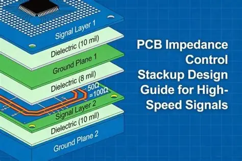
PCB stackup for impedance forms the foundation of these designs. The arrangement of signal layers, reference planes, and dielectric materials determines the electromagnetic field distribution around each trace. Proper stackup planning accounts for trace width, copper thickness, dielectric constant, and spacing to achieve the desired impedance. Gaming motherboards and graphics cards often employ six to twelve layer constructions to separate high-speed signals from power and ground planes while providing adequate return paths.
Technical Principles of High-Speed PCB Impedance
Impedance arises from the geometry and materials surrounding a conductor. In microstrip configurations, traces sit on the outer layers above a reference plane, with air or solder mask above. Stripline traces reside between two reference planes inside the board, offering better shielding but requiring tighter manufacturing tolerances. The impedance value depends on the ratio of trace width to dielectric height, the dielectric constant of the insulating material, and the presence of adjacent conductors.
Factors that influence impedance include variations in dielectric thickness, copper etching accuracy, and glass weave effects in the substrate. These variations can shift impedance by several ohms if not controlled during fabrication. Differential pairs require matched lengths and consistent spacing to maintain common-mode rejection and minimize electromagnetic interference. At frequencies typical in gaming hardware, even small discontinuities such as vias or connectors can create reflections that degrade eye diagrams and increase bit error rates.
Industry standards guide these calculations and verification processes. IPC-2141 provides design formulas and considerations for achieving controlled impedance in high-speed circuit boards. Designers use these guidelines alongside electromagnetic simulation to predict performance before committing to a physical layout.
Practical Solutions and Best Practices for Controlled Impedance Routing
Effective impedance matching techniques begin with early collaboration between design and fabrication teams. Engineers define target impedance values, tolerances, and test structures in the fabrication drawings. They specify the exact stackup, including material types and thicknesses, so that fabricators can adjust trace widths and spacings accordingly. This pre-planning reduces the need for multiple prototype iterations.
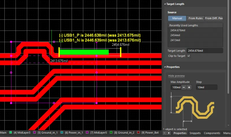
Routing practices emphasize continuous reference planes beneath high-speed traces and avoidance of unnecessary layer transitions. When vias are required, back-drilling or the use of blind and buried vias minimizes stubs that act as impedance discontinuities. Differential pair routing maintains equal lengths and consistent separation throughout the path, including through connectors and across board edges. Trace width adjustments compensate for changes in dielectric height or proximity to other features.
Material selection plays a critical role. Substrates with stable dielectric constants across temperature and frequency ranges help maintain impedance consistency during operation. Manufacturers verify the final product using test coupons that replicate the critical structures. Measurements confirm that actual impedance falls within the specified tolerance, commonly plus or minus ten percent for many gaming applications.
Conclusion
Mastering impedance in gaming PCB applications requires systematic attention to stackup design, trace geometry, and material properties. These practices ensure that high-speed signals propagate without distortion, supporting the performance expectations of modern gaming hardware. Engineers who integrate controlled impedance routing from the initial concept stage achieve more predictable results and fewer post-fabrication adjustments. Continued adherence to established design guidelines supports ongoing advances in signal speed and density.
FAQs
Q1: What defines pcb impedance control in gaming applications?
A1: PCB impedance control in gaming applications involves designing traces and stackups so that characteristic impedance matches system requirements, typically 50 ohms single-ended or 90 to 100 ohms differential. This matching minimizes reflections and preserves signal integrity across high-speed interfaces such as PCIe and memory buses. Consistent control supports reliable data transfer at the elevated clock rates found in gaming hardware.
Q2: How does controlled impedance routing improve high-speed PCB performance?
A2: Controlled impedance routing maintains uniform opposition to current flow along signal paths by specifying trace dimensions and reference plane placement. This uniformity reduces reflections and crosstalk that would otherwise distort waveforms. In gaming systems, the technique helps sustain maximum bandwidth and low latency during graphics-intensive operations.
Q3: Why is pcb stackup for impedance critical in multilayer designs?
A3: PCB stackup for impedance determines the electromagnetic environment around each trace through the positioning of signal layers, ground planes, and dielectric thicknesses. Accurate stackup planning allows precise calculation of trace widths needed to achieve target impedance values. Proper construction also provides continuous return paths that limit noise coupling in dense gaming boards.
Q4: What impedance matching techniques are used in high-speed designs?
A4: Impedance matching techniques include adjusting trace width and spacing according to dielectric properties, maintaining matched lengths for differential pairs, and incorporating series resistors or termination networks where necessary. Simulation tools verify that the implemented geometry produces the intended impedance before fabrication. Test coupons then confirm compliance after manufacturing.
References
IPC-2141A — Design Guide for High-Speed Controlled Impedance Circuit Boards. IPC.
IPC-2221 — Generic Standard on Printed Board Design. IPC.
IPC-6012E — Qualification and Performance Specification for Rigid Printed Boards. IPC, 2017.





