 ALLPCB


Why BMS Failure Mitigation Matters for Electric Engineers
A battery management system failure can lead to reduced battery life, unexpected downtime, or safety hazards in high-energy environments. Failure analysis of the associated PCB helps identify root causes such as trace degradation, via fatigue, or component misalignment before they propagate. For electric engineers working on electric vehicles, grid storage, or industrial packs, proactive mitigation reduces warranty claims and supports compliance with performance expectations. Structured approaches to PCB integrity directly influence the overall dependability of the battery management system.
Technical Principles and Common Causes of Failures
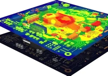
PCB failures in battery management systems often originate from thermal cycling, mechanical stress, or environmental exposure. Repeated temperature swings cause differential expansion between copper traces, laminate materials, and mounted components, leading to cracked solder joints or delaminated layers. High current paths for cell balancing can generate localized heating that accelerates electromigration or insulation breakdown when design margins are insufficient. Moisture ingress through imperfect coatings or poorly sealed connectors promotes corrosion on fine-pitch traces and sensor inputs, distorting voltage readings critical to the battery management system.
Electromagnetic interference represents another mechanism. Switching noise from balancing MOSFETs or communication buses can couple into sensitive analog measurement lines, producing erroneous state-of-charge calculations. Via fatigue under vibration becomes pronounced in mobile applications, where cyclic mechanical loads eventually open plated through-holes. Component-level issues such as moisture-induced popcorning during reflow further compound risks when boards are not handled according to established handling protocols.

Practical Solutions and Best Practices
Designers achieve robust mitigation through careful layout practices that separate high-current power planes from precision analog sections. Adequate copper weight on power traces, combined with thermal vias to internal planes or heatsinks, limits temperature rise and extends solder joint life. Redundant measurement paths and watchdog timers provide graceful degradation if a primary sensing circuit experiences an intermittent fault. Controlled impedance routing for communication lines reduces susceptibility to noise while maintaining signal integrity across the battery management system.
Manufacturing controls further strengthen reliability. Boards should undergo incoming inspection for laminate integrity and copper thickness uniformity. Solder paste application and reflow profiles must be validated to avoid voids or bridges on fine-pitch devices. Post-assembly testing includes in-circuit verification of all voltage sense lines, current shunt accuracy, and communication functionality under simulated load conditions. Environmental stress screening, such as temperature cycling and vibration, reveals latent defects before deployment.
Quality acceptance criteria aligned with IPC-A-600K help ensure that visual and dimensional characteristics meet requirements for high-reliability assemblies. Design rules following IPC-6012E provide qualification benchmarks for rigid boards used in demanding applications, guiding minimum annular ring sizes, via fill requirements, and material performance specifications.
Additional Insights on Testing and Validation
Failure analysis workflows typically begin with non-destructive techniques such as X-ray inspection for hidden solder defects and thermal imaging under load. When anomalies appear, cross-sectioning and scanning electron microscopy isolate the precise failure site, whether it is a cracked via barrel or corroded trace. Data from these analyses feed back into design iterations, tightening spacing rules or specifying higher glass-transition temperature laminates where needed. Continuous monitoring of field returns allows engineers to correlate laboratory findings with real-world usage patterns and refine mitigation strategies accordingly.
Conclusion
Battery management system failure mitigation relies on disciplined PCB design, controlled manufacturing, and systematic validation. By addressing thermal, mechanical, and electrical stress factors early, electric engineers can enhance the reliability of voltage monitoring, balancing, and protection functions. Adherence to established qualification and acceptability standards supports consistent outcomes across production lots. Ongoing failure analysis closes the loop between observed issues and design improvements, ultimately contributing to safer and more durable battery systems.
FAQs
Q1: What are the primary causes of failure in a battery management system PCB?
A1: Common causes include thermal cycling that induces solder joint fatigue, moisture ingress leading to corrosion on sense lines, and electromagnetic interference that distorts voltage measurements. Mechanical vibration can also fatigue vias in mobile applications. Thorough failure analysis helps pinpoint these issues before they affect overall battery management system performance.
Q2: How does PCB design influence battery management system reliability?
A2: PCB layout decisions such as trace width, via placement, and ground plane separation directly affect heat dissipation and noise immunity. Proper thermal relief patterns and redundant sensing paths reduce the likelihood of localized overheating or measurement errors. Following structured design practices minimizes the risk of failures that could compromise cell protection functions.
Q3: What role does failure analysis play in improving battery management system PCBs?
A3: Failure analysis identifies root causes through techniques like thermal imaging, cross-sectioning, and electrical testing. Insights gained allow engineers to adjust layouts, material selections, or assembly processes. This iterative approach strengthens future designs and reduces recurrence of similar issues in production battery management systems.
Q4: Which industry standards guide PCB quality for battery management systems?
A4: Standards such as IPC-6012E and IPC-A-600K establish qualification and acceptability criteria for rigid printed boards used in these applications. They cover aspects including material performance, dimensional tolerances, and visual inspection requirements that support consistent reliability in battery management system assemblies.
References
IPC-6012E - Qualification and Performance Specification for Rigid Printed Boards. IPC, 2017
IPC-A-600K - Acceptability of Printed Boards. IPC, 2020
JEDEC J-STD-020E - Moisture/Reflow Sensitivity Classification. JEDEC, 2014


