 ALLPCB


Why PCB Testing Matters for Battery Charger Designs
Battery charger PCBs handle high currents, voltage regulation, and thermal loads that demand precise control. Without comprehensive PCB testing, latent issues such as poor solder joints or incorrect component placement can lead to overheating or charging inefficiencies. Functional testing evaluates the complete assembly by simulating actual operating conditions, while in-circuit testing checks individual components before full integration. Automated testing systems increase throughput and repeatability in production environments. Safety testing focuses on protection circuits that prevent overvoltage, overcurrent, and short-circuit events. Compliance testing confirms that boards meet applicable industry expectations for electrical and mechanical performance.
Core Testing Methodologies and Their Applications
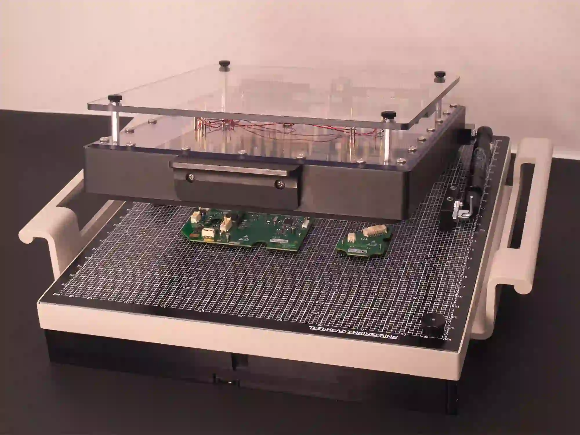
In-circuit testing uses a bed-of-nails fixture to probe nodes across the board and verify continuity, resistance, and basic component values. This method excels at catching manufacturing defects such as opens, shorts, and wrong-value parts before functional operation begins. Functional testing then applies power and input signals to confirm that the charger regulates voltage and current as specified. Automated testing platforms combine these steps with software-driven sequences that log results for traceability. Safety testing incorporates hipot, insulation resistance, and ground continuity checks to verify isolation between high-voltage and low-voltage sections. Compliance testing integrates these activities into a documented workflow that supports quality management systems.
Technical Principles of Effective Validation
Validation begins with understanding how electrical and thermal stresses interact within the charger circuit. Power semiconductors, inductors, and capacitors experience repeated cycling that can degrade solder joints or cause delamination if materials are not properly matched. In-circuit testing applies low-level signals to isolate component behavior without powering the full circuit, reducing the chance of damage during early screening. Functional testing then exercises the control loop, feedback network, and protection mechanisms under varying load conditions. Automated testing sequences allow engineers to repeat these checks with consistent timing and measurement accuracy. Thermal imaging during safety testing reveals hot spots that indicate inadequate copper weight or poor thermal via placement.
Best Practices for Reliable Test Implementation
Engineers begin by defining test coverage goals based on the criticality of each circuit section. High-current paths and protection components receive priority during in-circuit testing to catch placement or soldering issues early. Test fixtures must accommodate board warpage tolerances to maintain reliable probe contact across production batches. Automated testing programs incorporate boundary-scan techniques where available to improve fault isolation on dense layouts. Safety testing protocols follow a staged approach that starts with low-voltage checks before applying full operating voltages. Documentation of test limits, pass criteria, and failure modes supports traceability and continuous improvement of the validation process.

Compliance and Safety Integration in the Validation Flow
Adherence to IPC-6012E provides the qualification framework for rigid printed boards used in battery charger applications. This standard outlines acceptance criteria for conductor width, spacing, and via quality that directly affect electrical performance. Later in the process, reference to IPC-A-600K guides visual and dimensional inspection of finished boards to confirm they meet acceptability requirements. These guidelines help ensure that testing results reflect consistent manufacturing quality rather than variable board conditions.

Conclusion
Systematic PCB testing that combines in-circuit testing, functional testing, automated testing, safety testing, and compliance testing delivers the reliability and safety required for battery charger applications. Structured validation identifies defects at the earliest practical stage and confirms that protection circuits operate correctly under stress. Following established industry standards supports consistent quality across design iterations and production volumes. Engineers who implement these practices reduce field failures and support the performance expectations of electric vehicle, consumer, and industrial systems.
FAQs
Q1: What role does in-circuit testing play in battery charger PCB validation?
A1: In-circuit testing verifies individual components and connections on battery charger PCBs before full power is applied. It detects manufacturing defects such as opens, shorts, and incorrect component values that could compromise charging performance. This early screening complements later functional testing and helps maintain overall production yield.
Q2: How does functional testing differ from automated testing for battery charger PCBs?
A2: Functional testing applies real operating conditions to confirm that the complete battery charger circuit regulates voltage and current correctly. Automated testing uses programmed sequences and fixtures to execute both in-circuit and functional checks with high repeatability. Together they provide comprehensive coverage while improving efficiency in high-volume manufacturing.
Q3: Why is safety testing essential during compliance testing of battery charger PCBs?
A3: Safety testing evaluates isolation, hipot performance, and protection mechanisms that prevent hazards such as overvoltage or short circuits. When integrated into compliance testing, it confirms that the board meets the electrical and mechanical criteria outlined in relevant standards. This step supports safe operation across the expected temperature and load ranges.
Q4: What considerations guide the selection of test methods for battery charger PCB designs?
A4: Engineers evaluate board complexity, component density, and the presence of high-current paths when choosing between in-circuit testing, functional testing, and automated testing approaches. Safety testing and compliance testing are added based on the application environment and applicable industry expectations. The goal remains consistent validation that supports long-term reliability without introducing unnecessary process steps.





