 ALLPCB


Understanding Vias and Backdrilling in PCB Design
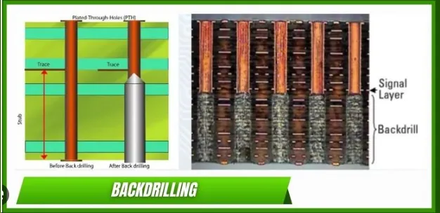
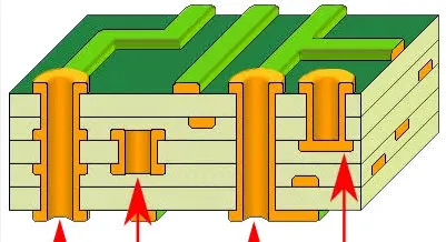
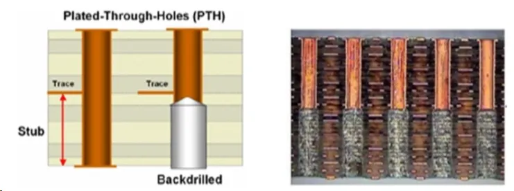
A via provides an electrical connection between layers in a multilayer printed circuit board. Traditional through vias extend fully from the top to the bottom surface, creating an unused stub portion beyond the intended connection layer. This stub can introduce impedance discontinuities that affect signal quality at elevated frequencies. Backdrilling removes the conductive plating from the unused stub after initial drilling and plating, leaving a controlled shorter via barrel. The technique applies primarily to high-speed differential pairs and single-ended nets where reflection and crosstalk must remain within acceptable limits.
The relevance of these choices grows as data rates increase in telecommunications, computing, and automotive electronics. Designers must balance the performance gains from stub removal against the incremental fabrication steps required. Procurement teams similarly evaluate how via decisions affect total project budgets and lead times. Industry standards such as IPC-6012E guide the qualification of rigid printed boards, including via formation and plating integrity, regardless of whether backdrilling is employed.
Technical Principles of Signal Propagation and Via Structures
Signal integrity depends on maintaining consistent characteristic impedance along the transmission path. In a traditional via, the unused barrel segment acts as a transmission line stub that reflects portions of the incident wave, particularly when the stub length approaches a quarter wavelength at the operating frequency. This reflection increases insertion loss, jitter, and bit-error rates in serial links. Backdrilling shortens the effective stub length, reducing the magnitude and timing of these reflections.
The backdrilling process begins with standard mechanical or laser drilling followed by copper plating. A secondary drilling operation, typically performed from the opposite side, removes plating to a precise depth controlled by drill depth stops or optical alignment. Depth accuracy directly influences residual stub length and therefore the resulting signal integrity improvement. Manufacturing tolerances for drill depth and registration must remain tight to avoid damaging functional plating or creating new discontinuities.
Thermal and mechanical stresses during backdrilling require attention to board material properties and stack-up symmetry. Uneven copper distribution or excessive resin content can lead to localized warpage that affects subsequent drilling accuracy.
Cost Factors in Via Selection and Manufacturing
Traditional vias require fewer fabrication steps, resulting in lower direct processing costs and shorter cycle times. The absence of a secondary drilling operation reduces machine time, tooling wear, and inspection requirements. Yield considerations also favor simpler via structures when board thickness and layer count remain moderate. These factors contribute to favorable via cost comparison outcomes for designs operating below critical frequency thresholds.
Backdrilling introduces additional variables into the PCB design cost analysis. Secondary drilling requires dedicated equipment, precise depth programming, and extra quality checks to confirm stub removal without over-drilling. Material waste from removed plating and potential scrap from depth errors further influence total expense. However, the signal integrity cost benefits can offset these increases when backdrilling enables higher data rates on existing layer counts or reduces the need for additional board layers and connectors.
Design teams often perform a quantitative trade-off study that includes backdrilling cost estimates alongside expected improvements in eye opening and margin. Factors such as board size, via count per net, and production volume determine whether the performance advantage justifies the added expense. Early collaboration between design and manufacturing engineers helps identify the frequency at which backdrilling becomes economically viable.
Best Practices for Selecting Via Structures
Engineers begin by modeling the expected operating frequency and rise time to determine whether via stubs will produce unacceptable reflections. Simulation tools calculate the maximum allowable stub length based on target return loss and insertion loss specifications. When modeling indicates that traditional vias will meet requirements, the simpler structure remains the preferred choice for cost efficiency.
When simulation shows marginal or failing performance, backdrilling offers a targeted remedy without requiring a complete board redesign. Designers specify backdrill depth on fabrication drawings with appropriate tolerances and call out inspection criteria. Layer stack-up symmetry and copper balancing remain important to maintain flatness through the additional processing step.
Production volume influences the decision as well. Low-volume or prototype builds may tolerate higher per-unit backdrilling cost to achieve required performance, while high-volume programs seek to minimize every added operation. In either case, adherence to established qualification standards ensures consistent via reliability across both approaches.
Practical Design Considerations and Yield Optimization
Via aspect ratio limits apply equally to traditional and backdrilled structures, although backdrilling can sometimes relax the effective aspect ratio by shortening the plated barrel. Designers maintain recommended annular ring sizes and spacing rules to support reliable plating and drilling registration. Thermal relief patterns around vias require review when backdrilling is planned, as the secondary operation may interact with relief geometry.
Yield optimization involves monitoring drill bit wear, depth control repeatability, and post-process cleanliness. Residue from backdrilling can affect subsequent solder mask application or assembly processes if not properly managed. Statistical process control tracks these parameters to maintain consistent quality and predictable costs.
Conclusion
Backdrilling and traditional vias each present distinct cost and performance profiles. Traditional vias deliver lower fabrication expense and simpler processing when signal integrity requirements permit their use. Backdrilling adds measurable cost yet provides measurable improvements in high-frequency behavior that can justify the investment in demanding applications. Systematic modeling, adherence to IPC-6012E and IPC-A-600K requirements, and early manufacturing involvement enable informed decisions that optimize both signal integrity cost benefits and overall project economics.
FAQs
Q1: What drives the difference in backdrilling cost compared with traditional vias?
A1: Backdrilling requires a secondary precision drilling step after initial plating, increasing machine time, tooling, and inspection. Traditional vias complete in a single drill-and-plate sequence. The added operations raise direct processing expense, although the magnitude depends on via count, board thickness, and production volume.
Q2: How does via cost comparison influence overall PCB design cost analysis?
A2: Via selection affects layer count, material choices, and yield expectations. Traditional vias keep fabrication simpler and less expensive for moderate-speed designs. Backdrilling may allow fewer layers or higher performance on the same stack-up, shifting the total cost equation when signal integrity demands are high.
Q3: What signal integrity cost benefits result from choosing backdrilling?
A3: Removing the via stub reduces reflections and improves insertion loss and return loss at high frequencies. These improvements can increase operating margin, reduce the need for additional equalization components, or enable higher data rates without redesigning the board.
Q4: When should engineers consider backdrilling during the design phase?
A4: Engineers evaluate backdrilling once simulation shows that conventional via stubs will exceed target return-loss or jitter limits. Early modeling combined with manufacturing feedback identifies the frequency threshold where the performance gain justifies the incremental processing cost.
References
IPC-6012E: Qualification and Performance Specification for Rigid Printed Boards
IPC-A-600K: Acceptability of Printed Boards





