 ALLPCB


Silkscreen markings play a critical role in guiding assembly operators and supporting quality checks during surface mount technology processes. Incorrect font sizes can lead to placement errors, reduced readability after reflow, and complications during automated optical inspection. Engineers and procurement teams must balance legibility with design for manufacturability rules to prevent costly rework. Proper font selection supports reliable component orientation, polarity indicators, and reference designators without interfering with solder joints or component bodies.
Why Silkscreen Font Size Matters in SMT Assembly
Silkscreen, also called legend or nomenclature, provides essential visual information on printed circuit boards. In SMT assembly, font size directly influences how well markings survive the process and remain functional for technicians. Oversized fonts may overlap pads or traces, creating clearance violations that increase the risk of solder bridging or tombstoning. Undersized fonts can become illegible after solder mask application or thermal exposure, complicating manual inspection and troubleshooting.
These issues contribute to common PCB assembly errors when design rules are overlooked. Following established silkscreen DFM practices helps maintain process yield and reduces the chance of defects reaching the field. 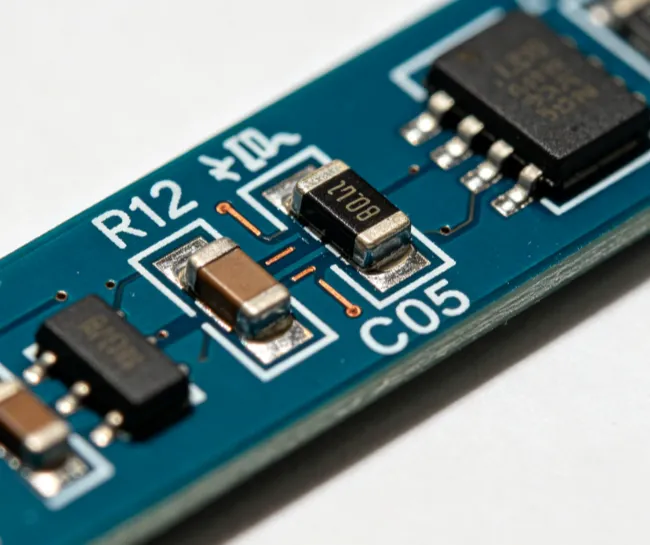
Technical Principles Behind Font Size Selection
Font height and stroke width determine both readability and physical compatibility with component footprints. Larger characters improve visibility for human operators during hand placement or rework, yet they demand greater clearance from pads and copper features. Smaller fonts conserve board space on dense layouts but risk disappearing under component bodies or becoming obscured by solder paste residue.
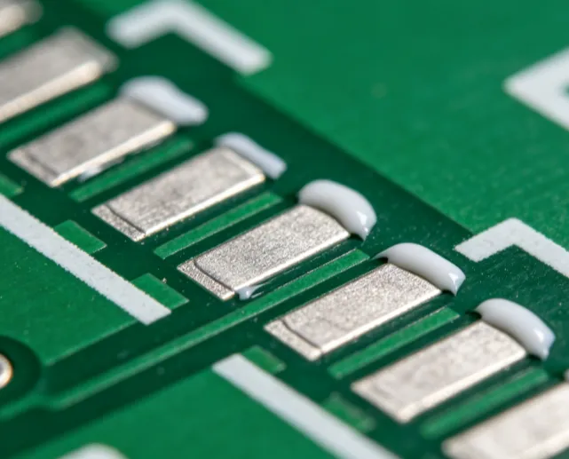
Clearance requirements between silkscreen and pads or traces are governed by manufacturing tolerances and assembly equipment capabilities. Insufficient clearance allows ink to migrate onto pad surfaces during printing, which can affect solder wetting and joint reliability. Industry standards such as IPC-A-610 provide acceptance criteria for marking quality after assembly, emphasizing that markings must remain intact and legible without compromising electrical performance.
Thermal cycling and reflow temperatures can also cause silkscreen ink to shift or fade if the font geometry is too fine. Designers therefore evaluate font size against the full thermal profile and the expected handling environment.
Practical Solutions and Best Practices for Silkscreen DFM
Begin by establishing minimum font height and width rules early in the layout phase. Reference designators and polarity marks should maintain consistent stroke thickness to avoid thin-line breakage during screen printing. Maintain adequate clearance from all pads, vias, and component outlines according to the fabricator’s and assembler’s DFM guidelines.
Review the board stack-up and solder mask registration tolerances before finalizing font sizes. Where space is limited, consider rotating text or using abbreviated markings rather than reducing font size below readable thresholds. Automated DFM checks within the design software can flag potential overlaps or insufficient clearances before files are released for fabrication.
Coordinate with the assembly house on their specific equipment limits for silkscreen resolution. Some processes allow finer features than others, so early communication prevents surprises during production. After first-article inspection, verify that all critical markings remain legible under the lighting conditions used for quality control. 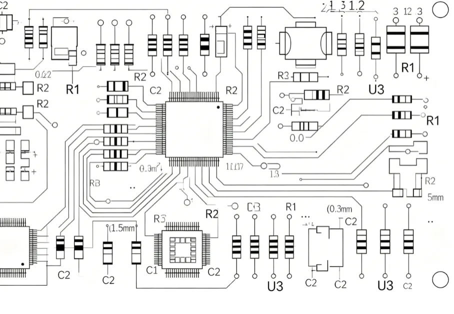
Troubleshooting Common Silkscreen Issues in SMT Production
When silkscreen disasters appear after assembly, the root cause often traces back to font size or placement decisions made during design. Blurred or missing text near components usually indicates insufficient clearance or ink spreading during the legend printing step. Operators may then struggle to confirm part orientation, leading to reversed components or missed rework.
If inspection systems flag low-contrast markings, increasing stroke width or selecting a higher-contrast ink color during fabrication can resolve the problem on subsequent builds. Persistent bridging near silkscreen often points to text that was placed too close to pads, allowing legend material to interfere with paste release. Revising the font size and repositioning text away from high-density areas typically restores yield.
Documenting these issues in a design checklist helps prevent recurrence across future projects. Regular review of assembled boards against the original layout files highlights whether font choices aligned with actual process capabilities.
Conclusion
Selecting the right silkscreen font size requires balancing readability, clearance, and process compatibility. Thoughtful application of silkscreen DFM principles reduces PCB assembly errors and supports consistent quality through SMT production. Early collaboration between design and manufacturing teams ensures that markings fulfill their intended purpose without introducing new risks.
FAQs
Q1: What are the key SMT assembly silkscreen guidelines for font size?
A1: Font height and stroke width must provide sufficient clearance from pads and component bodies while remaining legible after reflow and handling. Designers evaluate these dimensions against fabricator tolerances and assembly equipment limits to avoid ink migration or obscured markings. Following these guidelines supports reliable inspection and reduces the likelihood of placement mistakes during SMT assembly.
Q2: How does silkscreen over pads affect PCB assembly?
A2: Silkscreen over pads can deposit ink on surfaces intended for solder, interfering with paste adhesion and joint formation. This condition often results from oversized fonts or inadequate clearance rules during layout. Maintaining proper spacing prevents such interference and helps preserve solder joint integrity throughout the assembly process.
Q3: Why is silkscreen clearance important in DFM?
A3: Adequate clearance between silkscreen and copper features avoids bridging, tombstoning, and inspection failures. Clearance rules account for printing tolerances, mask registration, and thermal effects that can shift or spread legend material. Incorporating these considerations early in design improves overall manufacturability and yield.
Q4: What common PCB assembly errors result from poor silkscreen font choices?
A4: Errors include reversed components due to illegible polarity marks, solder bridging caused by ink on pads, and failed automated inspection from low-contrast or missing text. These issues typically stem from fonts that are either too large for available space or too small to survive processing. Addressing font size during DFM review helps eliminate these defects before production.
References
IPC-A-610H — Acceptability of Electronic Assemblies. IPC, 2020
J-STD-001H — Requirements for Soldered Electrical and Electronic Assemblies. IPC, 2020
IPC-6012E — Qualification and Performance Specification for Rigid Printed Boards. IPC, 2017





