 ALLPCB


Introduction
Aerospace PCBs face unique challenges due to extreme environmental conditions encountered during high-altitude operations. These boards must maintain trace integrity under rapid temperature changes, low pressure, intense vibration, and potential radiation exposure. Poor trace quality can lead to signal loss, intermittent failures, or complete system breakdowns, compromising mission safety and success. Electrical engineers designing for aerospace applications prioritize trace quality to ensure reliable performance from takeoff to high-altitude cruising or even space-adjacent missions. This article explores the critical aspects of aerospace PCB trace quality, focusing on standards, defects, and quality control measures tailored for high-altitude performance. By adhering to established PCB standards, manufacturers can deliver boards that withstand these rigors.

Why Trace Quality Matters in High-Altitude PCBs
High-altitude environments expose PCBs to reduced atmospheric pressure, which increases the risk of electrical arcing across traces if clearance distances are inadequate. Traces must resist cracking from thermal cycling, where temperatures swing from sub-zero to over 100 degrees Celsius in minutes. Vibration from engines and aerodynamics can propagate micro-cracks in traces, leading to opens over time. In aerospace PCBs, trace defects amplify under these stresses, potentially causing data corruption in avionics or power failures in control systems. Quality control becomes paramount to verify trace width, plating uniformity, and adhesion before deployment. Engineers must consider these factors during design to meet the demands of high-altitude PCB reliability.
Key Challenges for Trace Integrity in Aerospace Applications
Trace quality in aerospace PCBs hinges on precise etching, plating, and lamination processes that prevent defects exacerbated by high-altitude conditions. Low pressure reduces air dielectric strength, necessitating wider trace spacing to avoid partial discharges. Material expansion mismatches between copper traces and substrates can induce shear stresses during thermal excursions. Contaminants or voids trapped during fabrication migrate or grow under vacuum-like conditions, weakening traces. Vibration induces fatigue in plated layers, where thin or porous copper fails first. Addressing these requires factory processes aligned with high-reliability classes defined in PCB standards.
Common Trace Defects and Their High-Altitude Impacts
One prevalent trace defect is under-etching, where traces are narrower than specified, increasing resistance and heat generation during operation. Over-etching creates thin traces prone to necking and breakage under mechanical stress. Plating voids or pits in copper traces lead to electromigration acceleration in high-current paths, critical for power distribution in aerospace systems. Mouse bites, small nicks along trace edges, serve as crack initiation sites under vibration. Slivers, tiny copper particles from etching, can cause shorts if not removed. In high-altitude PCBs, these defects manifest faster due to thermal cycling and low pressure, underscoring the need for rigorous inspection.
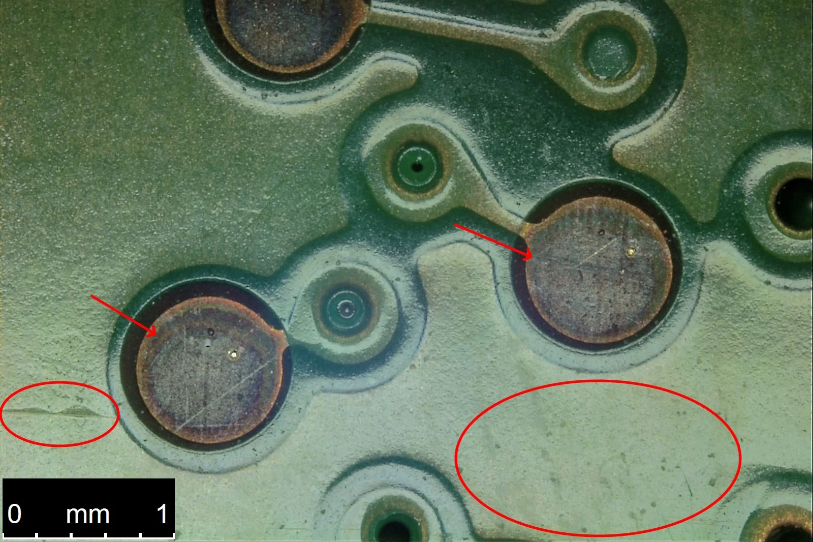
Cross-section analysis often reveals delamination at trace-substrate interfaces, stemming from poor adhesion or moisture entrapment. Pinholes in plating expose base copper to corrosion, worsened by outgassing in vacuum. Floating copper islands from incomplete etching bridge traces under flexing. These defects compromise signal integrity in high-speed data lines essential for radar and navigation. Factory-driven quality control identifies them early, preventing field failures.
PCB Standards Governing Aerospace Trace Quality
Aerospace PCBs typically require Class 3/A compliance, demanding enhanced trace surface quality and dimensional tolerances. IPC-6012DS provides specific qualification criteria for rigid boards in space and military avionics, including stringent trace etch control and plating thickness. This standard supplements general rigid board specs with vibration and thermal shock tests simulating high-altitude stresses. IPC-A-600M outlines acceptability criteria for traces, such as maximum allowable dents, roughness, and halos around conductors. These standards ensure traces maintain electrical and mechanical performance without adjacent repeats in verification.
Quality Control Processes for Trace Excellence
Quality control in aerospace PCB manufacturing starts with incoming material inspection for laminate cleanliness and copper foil uniformity. Automated optical inspection (AOI) scans for trace width variations, alignment, and surface anomalies post-etching. Electrical continuity testing verifies no opens or shorts under nominal conditions. Microsectioning samples traces for plating thickness, void content, and adhesion pull strength. X-ray imaging detects subsurface voids in buried traces. These steps align with factory protocols to certify high-altitude PCB readiness.
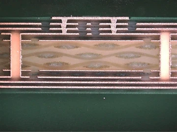
Flying probe or bed-of-nails testers apply voltage stress to check for dielectric weakness between traces. Thermal cycling per standard profiles simulates high-altitude excursions, monitoring resistance changes. Vibration tables replicate flight dynamics to assess fatigue. Data logging tracks defect rates, targeting near-zero escapes. Engineers review SPC charts for process stability, adjusting etchants or plating baths as needed.
Best Practices for Manufacturing High-Altitude PCBs
Select low-CTE substrates to minimize trace stress from thermal mismatch. Implement panel-level plating for uniform trace coverage, avoiding barrel cracks in vias adjacent to traces. Use plasma cleaning pre-lamination to enhance adhesion. Control etch factor to achieve vertical sidewalls, reducing undercut. Post-etch rinse thoroughly to eliminate slivers and residues. Bake boards to remove moisture before final assembly.
Design traces with generous annular rings and smoothed corners to resist cracking. Employ impedance-controlled routing for signal traces, verified by TDR. Conduct 100% AOI coupled with targeted microsections. Certify processes to quality management systems like ISO 9001:2015 for consistent output. These practices ensure aerospace PCB trace quality meets stringent standards.
Advanced Testing for High-Altitude Reliability
High-altitude simulation chambers combine low pressure, thermal ramps, and humidity to stress traces. Partial discharge testing under reduced pressure confirms creepage adequacy. Acoustic microscopy detects delams beneath traces. Solderability preservation post-fabrication prevents trace oxidation. These tests validate performance before integration.
Conclusion
Achieving superior trace quality in aerospace PCBs demands adherence to PCB standards, meticulous quality control, and proactive defect mitigation. High-altitude conditions amplify trace vulnerabilities, making factory insights essential for reliability. By focusing on etching precision, plating integrity, and environmental testing, engineers can deliver boards that perform flawlessly. Implementing these strategies minimizes trace defects and ensures mission-critical performance. Prioritizing these elements positions high-altitude PCBs for success in demanding applications.
FAQs
Q1: What are the most common trace defects in aerospace PCBs?
A1: Trace defects like under-etching, mouse bites, plating voids, and slivers compromise aerospace PCB integrity. These arise from etching imbalances or plating inconsistencies and worsen under high-altitude vibration and thermal cycling. Quality control via AOI and microsectioning detects them early. Adhering to IPC-A-600M criteria ensures acceptability for high-reliability use.
Q2: How do high-altitude conditions affect PCB trace quality?
A2: Reduced pressure at high altitudes increases arcing risk, requiring larger trace clearances. Thermal cycling induces fatigue cracks, while vibration propagates defects. Low air density hampers heat dissipation, overheating narrow traces. Robust quality control and standards like IPC-6012DS mitigate these for high-altitude PCB performance.
Q3: What PCB standards apply to aerospace trace quality control?
A3: IPC-6012DS and IPC-A-600M govern aerospace PCB trace specifications, defining Class 3/A criteria for etch control and surface quality. These ensure traces withstand high-altitude stresses. Factories use them for inspection and qualification, focusing on dimensional accuracy and defect limits.
Q4: How can engineers improve trace quality in high-altitude PCBs?
A4: Select matched CTE materials, optimize etching for uniform traces, and perform comprehensive testing like thermal vacuum cycling. Implement AOI, X-ray, and continuity checks in quality control. Follow PCB standards to guide processes, reducing defects for reliable high-altitude performance.





