 ALLPCB


Why Solder Mask Adhesion Matters in PCB Production
The solder mask layer must remain securely attached throughout thermal cycling, mechanical handling, and exposure to fluxes or cleaning chemistries. Delamination creates pathways for moisture ingress that accelerate corrosion and can cause intermittent opens or shorts. Factory processes are designed around consistent adhesion because rework after assembly is far more expensive than prevention at the coating stage. Standards such as IPC-6012E establish performance criteria that include adhesion testing to qualify boards for their intended end-use environments. When adhesion meets these criteria, boards exhibit improved yields during soldering operations and reduced warranty claims.
Primary Causes of Poor Solder Mask Adhesion
Contamination on the copper surface is one of the most frequent contributors to adhesion failure. Residues from previous processing steps, including oils, fingerprints, or oxidation layers, interfere with the chemical bonding that occurs during coating application. Inadequate surface preparation leaves these contaminants in place and reduces the effective contact area between the mask and the metal.
Moisture absorption in the substrate or laminate can also create vapor pressure during subsequent thermal excursions, lifting the mask at interfaces. Warpage induced by uneven heating or material mismatch further stresses the bond line.
Curing parameters that deviate from recommended profiles, such as insufficient ultraviolet exposure or incorrect oven temperatures, leave the polymer incompletely cross-linked. Under-cured material exhibits lower cohesive strength and poorer interfacial adhesion. Process variations in coating thickness or application method can compound these issues by creating stress concentrations at edges or vias.
Process Controls That Influence Adhesion Outcomes
Maintaining cleanroom-level cleanliness between etching and solder mask application minimizes particulate and chemical contamination. Plasma or chemical cleaning steps remove oxides and organic films, restoring a high-energy surface that promotes wetting and bonding. Monitoring the time between cleaning and coating prevents re-oxidation that would otherwise degrade results.
Curing ovens and ultraviolet lamps require regular calibration to ensure uniform energy delivery across panels. Recording actual exposure times and temperatures for each batch allows traceability when adhesion issues arise. Thickness measurements at multiple locations confirm that the mask meets minimum build requirements without excessive buildup that could trap solvents.
Incoming material inspection verifies that laminate moisture content remains within acceptable limits before processing begins. Controlled storage environments and pre-bake cycles reduce absorbed water that could later expand during reflow. Statistical process control tracks key variables such as surface energy after cleaning and cure degree after exposure, providing early warning of drift.

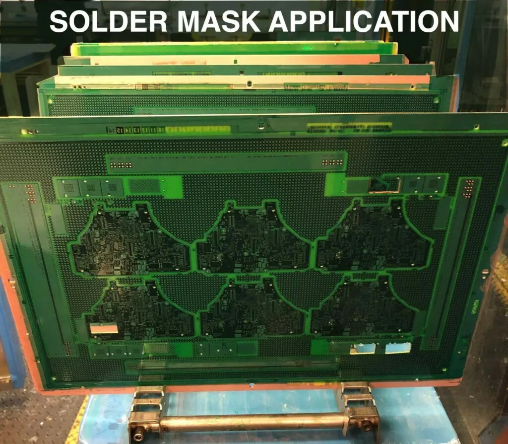
Best Practices for Reliable Solder Mask Application
Engineers specify adhesion testing methods aligned with IPC-A-600K acceptance criteria during incoming or in-process inspection. Cross-hatch or tape-pull evaluations performed on representative panels confirm that the coating withstands handling stresses. When results fall short, root-cause analysis focuses on the most recent process step before the defect was detected.
Collaboration between design and manufacturing teams ensures that layout features such as large copper pours or dense via fields receive appropriate mask coverage without creating adhesion-compromising geometries. Process documentation captures approved parameters for each board type, enabling consistent replication across production runs. Regular audits of cleaning chemistry concentration and filtration effectiveness maintain surface preparation quality over time.
Troubleshooting Recurring Adhesion Issues
When adhesion problems appear repeatedly on the same product family, teams review the full process history for changes in chemistry suppliers, equipment maintenance schedules, or environmental conditions. Moisture-related failures often correlate with seasonal humidity spikes or extended storage before coating. Adjusting pre-bake protocols or improving dry-box storage frequently resolves these patterns.
Curing-related defects may trace to lamp degradation or conveyor speed variations. Verifying energy output with calibrated radiometers and confirming dwell times restores consistent cross-linking. In cases involving substrate warpage, finite-element analysis of the stack-up helps identify material combinations that minimize differential expansion.
Conclusion
Consistent solder mask adhesion depends on disciplined surface preparation, precise curing control, and ongoing process monitoring. Electrical engineers who incorporate these elements into PCB specifications reduce the likelihood of delamination and associated reliability risks. Adherence to recognized industry standards provides a common framework for qualification and acceptance that supports both prototype and volume production needs.
FAQs
Q1: What steps improve solder mask adhesion on copper surfaces?
A1: Effective surface preparation through plasma or chemical cleaning removes oxides and contaminants before coating. Controlled timing between cleaning and application, combined with verified curing profiles, ensures strong interfacial bonding. Regular monitoring of surface energy and cure degree supports consistent results across batches.
Q2: How does improper curing affect solder mask adhesion?
A2: Insufficient ultraviolet exposure or incorrect thermal profiles leave the polymer under-cross-linked, reducing both cohesive strength and bond integrity. Over-curing can embrittle the material and create stress points. Maintaining calibrated equipment and documented process parameters minimizes these risks.
Q3: Why is PCB cleaning critical for preventing poor solder mask adhesion?
A3: Residual contaminants block direct contact between the mask and the substrate, preventing chemical adhesion. Thorough cleaning restores surface wettability and removes films that would otherwise cause lifting during thermal or mechanical stress. Process control of cleaning chemistry and rinse quality maintains effectiveness.
Q4: What role does process control play in solder mask quality?
A4: Process control tracks variables such as coating thickness, cure energy, and substrate condition to detect deviations before they produce defective boards. Statistical monitoring and documented parameters enable rapid corrective action when trends appear. This approach aligns with factory-driven quality systems that emphasize prevention over rework.


