 ALLPCB


Target impedance plays a central role in modern PCB design. Engineers define a specific impedance value for critical traces to ensure signals propagate correctly without excessive reflection or distortion. This value becomes the foundation for impedance planning throughout the PCB design process. When target impedance aligns with signal integrity requirements, the overall system performs reliably across operating frequencies. Proper impedance planning reduces the risk of signal degradation in high speed applications. It also supports consistent manufacturing outcomes when boards move into production.
What Is Target Impedance and Why It Matters
Target impedance refers to the desired characteristic impedance of a transmission line on a printed circuit board. Designers calculate this value early in the PCB design process based on driver and receiver specifications. Typical single ended values often fall in the 50 ohm range while differential pairs commonly target 90 or 100 ohms. Establishing a clear target impedance allows the team to create an impedance budget that allocates tolerances across the entire interconnect path. This budget accounts for variations in trace geometry, dielectric materials, and manufacturing tolerances. Without a defined target, signal integrity requirements become difficult to verify during layout and testing.
The importance of target impedance extends beyond basic functionality. It directly influences electromagnetic compatibility and power integrity in complex boards. When impedance mismatches occur, reflections can degrade rise times and increase crosstalk between adjacent traces. In multilayer designs, consistent impedance also supports reliable operation at higher data rates. Industry standards such as IPC 2221 provide guidance on design practices that help maintain controlled impedance across production lots. Meeting these requirements early avoids costly respins later in the project.
Technical Principles of Impedance in PCB Layout
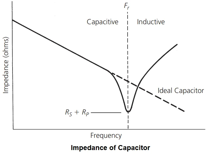
Impedance arises from the interaction of inductance and capacitance along a conductor. Trace width, thickness, and spacing relative to reference planes determine the inductance per unit length. The dielectric constant and thickness of the insulating layers control the capacitance. Together these parameters produce the characteristic impedance that a signal experiences as it travels. In differential signaling, the coupling between the pair adds another dimension that must be modeled accurately. Small changes in any of these variables can shift the impedance outside acceptable limits.
An impedance budget breaks the total allowable deviation into individual contributors. Typical budgets allocate portions to etching tolerance, dielectric variation, and copper thickness. Designers then verify that the stackup and routing rules keep each contributor within its share of the budget. Simulation tools model the electromagnetic fields to predict the resulting impedance before fabrication. Measurement on test coupons after manufacturing confirms that the actual values fall within the planned range. This structured approach ensures that signal integrity requirements remain satisfied even when process variations occur.
Best Practices for Impedance Planning in the PCB Design Process
Effective impedance planning begins with a clear definition of signal integrity requirements during schematic capture. Engineers identify high speed nets and assign target impedance values based on interface standards and component datasheets. The next step involves collaboration with the fabricator to select a stackup that supports the required impedance with available materials. Trace geometry rules are then set in the layout tool so that width and spacing automatically produce the target value. Differential pair routing maintains consistent spacing and length matching to preserve the intended differential impedance.
Simulation at the pre layout and post layout stages validates the design against the impedance budget. Engineers adjust trace widths or reference plane assignments when simulations show deviations. Test structures placed on the panel allow impedance measurement after fabrication. These measurements confirm that the manufactured board meets the original target impedance within the allocated tolerance. Documentation of the impedance budget and stackup decisions supports traceability and future design reuse. Following these steps reduces the likelihood of signal integrity issues during system integration.
Conclusion
Target impedance serves as the foundation for successful high speed PCB design. Defining it early enables accurate impedance planning and alignment with signal integrity requirements. A well constructed impedance budget guides layout decisions and manufacturing tolerances. When these elements are managed together, boards achieve reliable performance and consistent production yields. Structured engineering practices ensure that target impedance remains a controllable parameter rather than an afterthought.
FAQs
Q1: How does target impedance influence the PCB design process?
A1: Target impedance sets the electrical goal for critical traces and guides stackup selection, trace geometry, and routing constraints. It forms the basis of the impedance budget that distributes allowable variations across design and manufacturing steps. Early definition of target impedance helps satisfy signal integrity requirements before layout begins.
Q2: What factors determine the impedance budget in a PCB project?
A2: The impedance budget accounts for variations in trace width, copper thickness, dielectric constant, and etching accuracy. Each contributor receives a portion of the total tolerance so that the final impedance stays within acceptable limits. This allocation supports consistent signal integrity across production boards.
Q3: Why is impedance planning important for signal integrity requirements?
A3: Impedance planning ensures that reflections and crosstalk remain within acceptable levels as signals travel across the board. When target impedance matches the system needs, rise times and voltage levels stay intact. Proper planning reduces the risk of timing errors and electromagnetic interference in the final assembly.
Q4: How do industry standards support target impedance control?
A4: Standards such as IPC 6012E define performance expectations for controlled impedance boards and outline qualification methods. They provide a common framework for designers and fabricators to agree on acceptable impedance ranges and test procedures. Compliance with these standards helps ensure repeatable results in volume production.


