 ALLPCB


Impedance control ensures consistent signal transmission in high-speed circuits. Variations during fabrication can lead to reflections, crosstalk, and performance degradation. Manufacturers address these challenges through structured process controls and verification steps that align with established industry practices. Effective troubleshooting begins with understanding how design intent translates into physical board characteristics.
Why Impedance Control Matters in PCB Manufacturing
Controlled impedance supports reliable data transfer rates in applications ranging from telecommunications to computing systems. Deviations from target values often stem from material and process variables that affect trace geometry and surrounding dielectrics. When tolerances are not maintained, signal integrity suffers, increasing the risk of system-level failures. Manufacturers therefore integrate impedance requirements into every stage from material selection through final inspection.
Industry standards such as IPC-6012E outline qualification requirements that include verification of electrical performance parameters. These guidelines help ensure boards meet functional expectations before assembly. Procurement teams and designers benefit from early collaboration with fabricators to define realistic targets that account for production capabilities.
Technical Principles Behind Impedance Variations
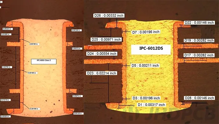
Impedance depends on the relationship between conductor dimensions, dielectric properties, and reference plane spacing. Small changes in copper thickness or substrate height can shift values outside acceptable ranges. Etching processes influence trace width and edge profiles, while lamination cycles affect dielectric consistency across panels. These interactions create cumulative effects that require precise monitoring.
Manufacturing defects such as inconsistent resin flow or foil irregularities contribute to localized impedance shifts. Warpage during thermal excursions can further alter effective spacing between layers. TDR testing reveals these anomalies by sending pulses along traces and analyzing reflection patterns that indicate mismatches. Systematic mapping of results helps isolate whether issues originate in design, materials, or fabrication steps.
Common Causes of Impedance Control Failures
Over-etching or under-etching alters conductor width beyond design specifications, directly impacting characteristic impedance. Variations in dielectric constant arise from batch-to-batch differences in substrate materials or improper storage conditions. Copper roughness on inner layers can increase effective resistance at higher frequencies, compounding the problem. Panel-level inconsistencies during pressing also lead to thickness gradients that affect multiple boards.
PCB quality control procedures must detect these issues before boards reach assembly. Without adequate checks, defects propagate into final products, raising scrap rates and delaying deliveries. Root-cause analysis typically examines process logs alongside test data to pinpoint the responsible variable.
Practical Solutions and Best Practices
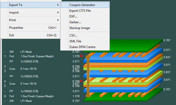
Design rules should incorporate manufacturer feedback on achievable tolerances for trace width, spacing, and dielectric thickness. Pre-production impedance modeling combined with coupon testing validates stack-up choices. During fabrication, automated optical inspection and in-process measurements maintain geometry within limits. Post-lamination verification confirms dielectric uniformity across the panel.
Impedance testing using TDR equipment provides quantitative data for each critical net. Results guide adjustments to etching chemistry or press parameters on subsequent lots. Statistical process control tracks trends and triggers corrective actions when measurements approach tolerance boundaries. Documentation of these controls supports traceability required by quality management systems.
Additional measures include controlled storage of raw materials to stabilize dielectric properties and calibrated equipment for all dimensional checks. Collaboration between design and manufacturing teams refines stack-up details to reduce sensitivity to normal process variation. These steps collectively minimize the occurrence of out-of-specification boards.
Troubleshooting Workflow from a Manufacturer's View
When impedance issues appear, the first step involves reviewing TDR data against design targets to determine deviation magnitude and location. Cross-sectional analysis then confirms actual geometry compared with nominal values. If trace widths prove inconsistent, etching parameters receive adjustment; if dielectric thickness varies, lamination recipes are examined.
Further investigation may include material certification review and environmental conditioning tests. Corrective actions are validated on pilot runs before full production resumes. This methodical approach reduces recurrence and improves overall yield.
Conclusion
Maintaining impedance control requires attention to multiple interdependent factors throughout the PCB manufacturing process. Structured testing, adherence to recognized standards, and iterative process refinement enable consistent results. Engineers who incorporate these practices early achieve better signal integrity and fewer downstream complications.
FAQs
Q1: What role does TDR testing play in PCB quality control?
A1: TDR testing measures impedance along transmission lines by analyzing reflected signals. It identifies deviations caused by manufacturing defects such as incorrect trace geometry or dielectric variations. Regular application during production helps maintain specified tolerance levels and supports reliable high-speed performance.
Q2: How do impedance tolerance requirements affect PCB manufacturing defects?
A2: Tight impedance tolerance limits increase sensitivity to small process variations in etching, lamination, and material properties. Manufacturers must apply tighter controls and more frequent verification to stay within bounds. This reduces the likelihood of defects that compromise signal integrity.
Q3: Why is impedance testing important for electric engineers designing high-speed boards?
A3: Impedance testing confirms that fabricated boards match design intent for characteristic impedance. It reveals issues that could cause reflections or attenuation before assembly. Engineers use the data to validate stack-ups and refine future layouts for better manufacturability.
Q4: What are typical steps in troubleshooting impedance issues during PCB fabrication?
A4: Troubleshooting begins with TDR measurements to locate mismatches, followed by cross-section analysis to check physical dimensions. Process parameters such as etch rates and press cycles are then reviewed and adjusted. Validation on subsequent lots ensures the corrective actions restore compliance.


