 ALLPCB


Introduction
Aerospace PCB design demands precision in every aspect, particularly the layer stackup, which forms the foundation of reliable electronics in extreme environments. High-altitude PCB operations expose boards to rapid thermal cycling, low pressure, and vibration, while space missions add radiation challenges that can degrade materials over time. Engineers must prioritize lightweight PCB constructions to meet strict weight budgets without compromising performance. The aerospace electronics stackup configuration directly influences signal integrity, power distribution, and mechanical stability. This article delves into the structured approaches for designing stackups that withstand these rigors, drawing on established engineering principles. By optimizing layer arrangements, designers ensure mission-critical systems operate flawlessly from takeoff to orbit.
Understanding Aerospace PCB Layer Stackup
Aerospace PCB layer stackup refers to the precise arrangement of copper layers, dielectrics, and cores that define a multilayer board's electrical, thermal, and mechanical properties. Unlike commercial PCBs, aerospace versions incorporate materials with enhanced thermal stability and dimensional consistency to handle high-altitude conditions. Radiation resistant PCB stackups often feature dielectrics that minimize charge trapping and outgassing under cosmic ray exposure. Lightweight PCB goals drive thinner cores and reduced layer counts where possible, balanced against routing density needs. Core principles include maintaining symmetry across the stack to prevent warpage during fabrication and assembly. Proper stackup planning aligns with IPC-2221 guidelines for generic printed board design, ensuring controlled impedance and minimal crosstalk.
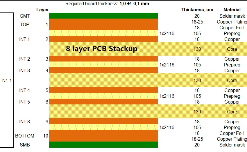
Engineers define stackup early in the design phase, specifying thicknesses, material types, and plane assignments. This step integrates constraints like high-speed signal propagation and EMI suppression critical for avionics. In high-altitude PCB applications, stackups must accommodate expansion mismatches between layers to avoid delamination from pressure differentials. Radiation resistant designs emphasize uniform dielectric properties to distribute stress evenly. Overall, the stackup serves as the blueprint for transforming conceptual circuits into robust hardware.
Why Aerospace Electronics Stackup Matters
Reliability in aerospace electronics stackup is non-negotiable, as failures can cascade into catastrophic outcomes during flight or satellite deployment. High-altitude PCB environments induce thermal gradients exceeding 100 degrees Celsius swings, stressing interlayer bonds and vias. Radiation resistant PCB requirements stem from single-event upsets and total dose effects that alter conductivity in standard materials. Lightweight PCB stackups reduce fuel costs and payload mass, yet demand higher layer densities for complex radar and navigation systems. Poor stackup choices amplify issues like signal skew, increasing bit error rates in data links. Thus, meticulous design prevents downtime and extends operational life in unforgiving conditions.
The economic stakes amplify the need for optimized aerospace PCB design. Redesigns or failures mid-mission incur millions in losses, underscoring stackup's role in qualification testing. Vibration from engines transmits through unbalanced stacks, causing micro-cracks in copper. Engineers leverage stackup symmetry to equalize CTE across planes, mitigating these risks. In summary, effective stackups bridge performance, weight, and durability for sustained aerospace superiority.
Key Technical Principles in Aerospace PCB Stackup Design
Material selection anchors aerospace PCB layer stackup, favoring laminates with low coefficient of thermal expansion and high glass transition temperatures for stability. Dielectrics must exhibit consistent permittivity to preserve controlled impedance across temperature extremes in high-altitude PCB scenarios. Radiation resistant PCB stackups prioritize materials resistant to ionization, reducing latch-up risks in active components. Copper weights balance conductivity with weight savings in lightweight PCB builds, often using 1 oz/ft2 foils for inner layers. Prepregs fill gaps precisely, ensuring adhesion under thermal shock.
Symmetry in layer pairing prevents bow and twist, a primary warpage mechanism during lamination. Outer signal layers flank ground planes to minimize loop inductance and EMI radiation. Power planes provide low-impedance returns, crucial for transient suppression in power-hungry avionics. Via structures, including blind and buried types, optimize density without penetrating the entire stack, preserving mechanical integrity. Thermal management integrates embedded planes and vias to dissipate heat from high-power devices.
Signal integrity principles dictate plane proximity; ground planes adjacent to high-speed traces form stripline configurations with predictable characteristic impedance. Aerospace electronics stackup often employs hybrid constructions, mixing high-frequency and RF layers for integrated systems. Mechanical robustness counters g-forces, with stackups designed for uniform thickness to distribute stresses. Fabrication tolerances tighten per IPC-6012DS space addendum requirements, validating performance under vibration and thermal cycling.
Best Practices for Designing Radiation Resistant and Lightweight Stackups
Start with requirements analysis, mapping layer functions to mission profiles like altitude, radiation dosage, and mass limits. Allocate ground and power planes alternately to create shielding and decoupling capacitance inherent in the stackup. For high-altitude PCB reliability, select dielectrics with low moisture absorption to prevent popcorning during ascent. Radiation resistant PCB designs incorporate redundant routing on inner layers, shielded by outer planes. Lightweight PCB stackups minimize core thicknesses while maintaining rigidity through core stitching vias.
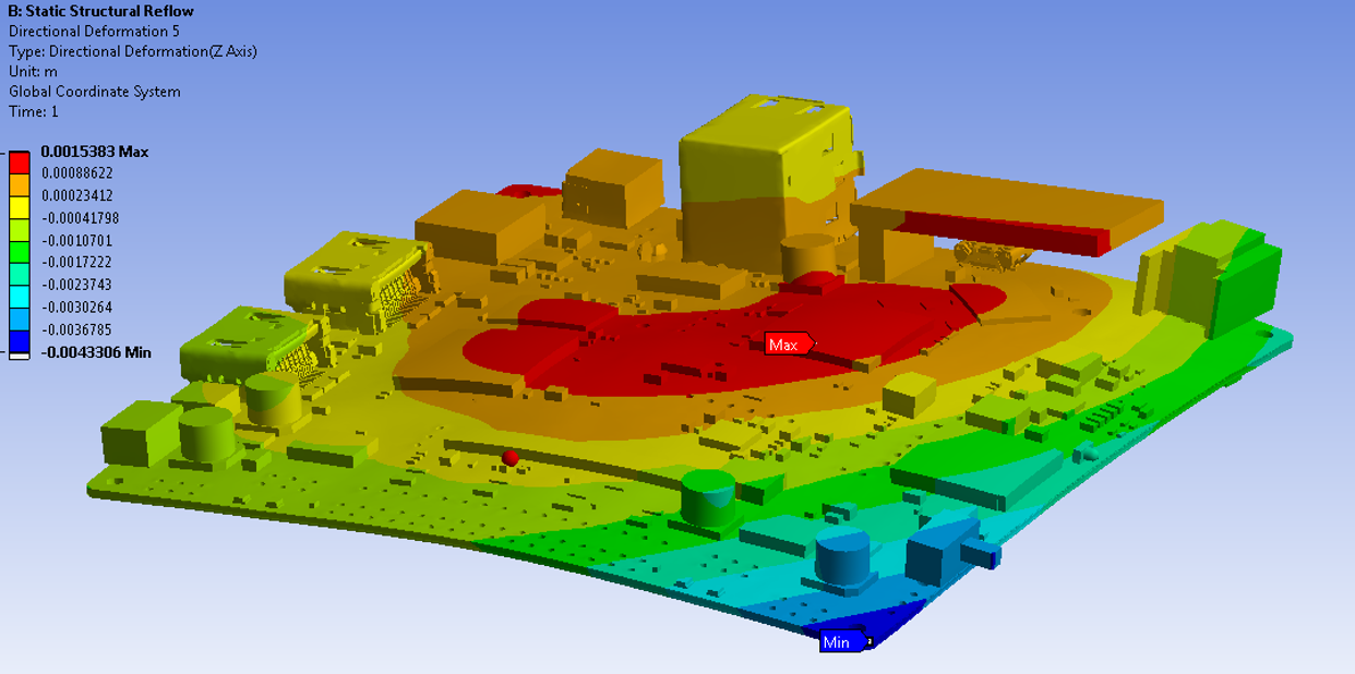
Impedance modeling tools simulate stackup performance, targeting 50-ohm singles and 100-ohm differentials for data buses. Balance copper distribution to avoid plating voids, adhering to J-STD-020 for handling sensitivity. Sequential lamination processes suit complex stacks, building subsections for better yield. Prototype testing verifies warpage below allowable limits post-reflow.
Vibration damping integrates via fences and plane splits judiciously, avoiding splits under high-current paths. For aerospace PCB design, document stackup with drill tables and material callouts for fabricator alignment. Iterative reviews incorporate DFM feedback, refining for manufacturability. These practices ensure stackups meet IPC-6012DS qualifiers for space avionics.
Troubleshooting Common Stackup Challenges in Critical Applications
Imbalanced stacks often manifest as warpage, detectable via shadow moiré interferometry during qualification. Asymmetric copper leads to CTE-induced bowing; remedy by mirroring layers top-to-bottom. Signal crosstalk in dense high-altitude PCB arises from insufficient plane separation; tighten dielectric control and add stitching vias. Radiation-induced degradation appears as increased leakage; mitigate with wider clearances and guard traces.
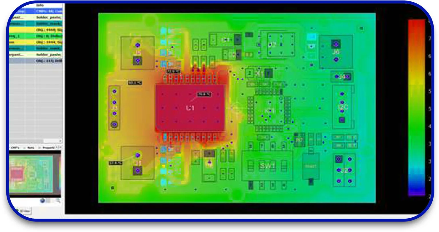
Thermal hotspots from poor plane coupling cause hotspots; redistribute power dynamically across planes. Lightweight PCB pursuits risk flexing under vibration; reinforce with edge clamps and thicker cores selectively. Fabrication defects like drill breakout stem from stackup misalignment; use positive etchback processes. Systematic root-cause analysis, paired with standards compliance, resolves these iteratively.
Conclusion
Aerospace PCB layer stackup design integrates material science, electromagnetics, and mechanics to deliver unparalleled reliability. High-altitude PCB challenges demand symmetric, thermally stable configurations, while radiation resistant PCB needs focus on material resilience. Lightweight PCB innovations enable efficient missions without sacrificing integrity. Aerospace electronics stackup best practices, grounded in logical layer planning, ensure signal fidelity and structural endurance. Engineers who master these principles produce boards ready for the extremes of flight and space. Prioritizing standards and simulation yields stackups that power the future of aviation.
FAQs
Q1: What key factors influence aerospace PCB design for high-altitude environments?
A1: High-altitude PCB stackups must address thermal cycling, low pressure, and vibration through symmetric layer arrangements and low-CTE materials. Ground planes adjacent to signals enhance EMI control and return paths. Dielectric choices prevent delamination, ensuring reliable operation above 30,000 feet. Balanced copper distribution minimizes warpage during pressure changes. These elements maintain performance in stratified atmospheres.
Q2: How does radiation resistant PCB stackup differ from standard designs?
A2: Radiation resistant PCB stackups use dielectrics with high radiation tolerance to resist total ionizing dose effects and single-event phenomena. Redundant inner layers shielded by planes reduce upset risks. Wider trace spacing accommodates potential conductivity shifts post-exposure. Uniform material properties distribute stress evenly. This configuration sustains functionality in cosmic ray-heavy orbits.
Q3: What strategies optimize lightweight PCB for aerospace electronics stackup?
A3: Lightweight PCB stackups employ thin cores, low-weight foils, and blind vias to cut mass while preserving density. Hybrid signal-power arrangements leverage plane capacitance for decoupling. Material selection favors density under 2 g/cm3 without strength loss. Symmetry ensures flatness for conformal coating. These tactics meet stringent payload limits in aircraft and satellites.
Q4: Why is layer symmetry critical in aerospace PCB design?
A4: Layer symmetry in aerospace PCB design counters warpage from CTE mismatches during lamination and thermal excursions. Balanced stacks maintain planarity for assembly and vibration resistance. It equalizes expansion, preventing via barrel cracks. IPC guidelines reinforce this for high-reliability classes. Resulting boards endure g-loads and cycles without deformation.
References
IPC-6012DS — Space and Military Avionics Applications Addendum to IPC-6012D, Qualification and Performance Specification for Rigid Printed Boards. IPC, 2015
IPC-2221 — Generic Standard on Printed Board Design. IPC, 1998
J-STD-020E — Moisture/Reflow Sensitivity Classification. JEDEC, 2014





