 ALLPCB


Advanced Via Stitching: Reducing EMI and Noise
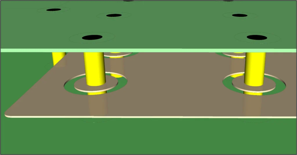
Via stitching involves placing multiple vias in a deliberate pattern to connect copper layers, particularly ground planes, within a printed circuit board. This technique creates low-inductance paths that help manage electromagnetic interference and unwanted noise in electronic designs. Engineers apply via stitching when signal integrity and electromagnetic compatibility become critical factors in multilayer boards. The approach supports stable return currents and minimizes loop areas that can radiate or pick up interference. Proper implementation requires careful planning of via size, spacing, and placement relative to signal traces and power planes.
What Is Via Stitching and Why It Matters
Via stitching refers to the systematic addition of vias that electrically connect separate ground or reference planes across different layers of a PCB. It improves the integrity of return paths for high-speed signals and reduces the impedance seen by those currents. In modern electronic systems operating at higher frequencies, even small inductances can lead to voltage drops or radiated emissions that affect overall performance. Via stitching addresses these issues by distributing current more evenly and lowering the effective inductance of the ground network. Industry standards such as IPC-2221 provide guidance on board design practices that support reliable via implementation in complex layouts.
The relevance of via stitching has grown with the proliferation of high-speed digital interfaces, RF circuits, and dense mixed-signal designs. Without adequate stitching, ground planes can behave as unintended antennas or resonators, amplifying noise that couples into sensitive analog sections. Engineers therefore evaluate via stitching early in the layout phase to meet electromagnetic compatibility requirements and ensure stable operation across temperature and voltage variations. This method also contributes to better thermal distribution in some cases by increasing the number of thermal pathways between layers.
Technical Principles of Via Stitching for EMI Reduction
The primary mechanism behind via stitching lies in reducing the inductance of return paths. Each via presents a small but measurable inductance that decreases when multiple vias operate in parallel. By spacing vias at intervals typically related to the wavelength of concern, designers create a more uniform ground plane that approximates a solid sheet at the frequencies of interest. This configuration limits the formation of large current loops that radiate electromagnetic energy. Signal improvement via vias occurs because cleaner return paths reduce crosstalk and preserve edge rates on digital signals.
Electromagnetic interference arises when rapidly changing currents generate magnetic fields that couple into nearby conductors. Via stitching confines these fields by providing numerous low-impedance routes back to the source. The result is lower radiated emissions and improved immunity to external fields. In boards with split planes or multiple ground domains, stitching helps maintain reference continuity without introducing new discontinuities that could reflect signals. Engineers often model these effects using electromagnetic simulation tools to verify that the chosen via pattern achieves the desired suppression across the operating bandwidth.
Practical Solutions and Best Practices for Via Design
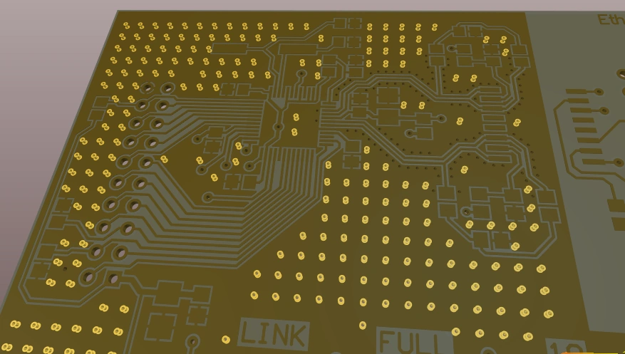
Effective via stitching begins with identifying critical return paths associated with high-speed or sensitive signals. Designers place vias along the edges of ground planes and near signal vias to ensure short, direct routes for return current. Via diameter, pad size, and plating thickness influence both inductance and current-carrying capacity, so these parameters receive attention during stack-up definition. Spacing between stitched vias commonly follows guidelines that keep the distance small relative to the highest frequency of interest, typically on the order of one-tenth of the wavelength or less.
Additional best practices include staggering via locations to avoid creating resonant structures and ensuring adequate clearance from signal traces to prevent unintended coupling. In regions with dense component placement, via stitching must balance EMI performance against routing density and manufacturing yield. Thermal relief connections around power vias can be combined with stitching patterns when heat dissipation is also a concern. Regular review of the layout against electromagnetic compatibility test requirements helps confirm that the via arrangement delivers measurable improvements in noise margins.
Considerations for High-Frequency and Mixed-Signal Applications
In radio-frequency and high-speed digital designs, via stitching supports controlled impedance environments by maintaining consistent reference planes. Discontinuities introduced by insufficient stitching can cause reflections that degrade signal quality and increase bit-error rates. Engineers therefore integrate via stitching with other layout techniques such as trace length matching and proper termination. When analog and digital sections share the same board, stitching helps isolate noisy digital return currents from sensitive analog ground areas.
Manufacturing considerations include drill aspect ratios and plating uniformity, which affect via reliability under thermal cycling. Standards such as IPC-6012 outline acceptance criteria for via structures that ensure long-term electrical and mechanical performance. Designers also evaluate the impact of via stubs in thick boards, sometimes opting for back-drilling or blind vias when stub resonances fall within the signal bandwidth. These choices form part of a broader strategy that combines via stitching with careful plane allocation and component placement.
Conclusion
Via stitching provides a practical and effective means of addressing electromagnetic interference and noise in printed circuit board designs. By creating multiple low-inductance connections between reference planes, engineers achieve better current distribution, reduced loop areas, and improved overall signal integrity. The technique integrates well with established design practices and supports compliance with electromagnetic compatibility expectations across a wide range of applications. Careful attention to via placement, sizing, and spacing during layout yields measurable benefits in both prototype and production boards.
FAQs
Q1: How does via stitching contribute to EMI reduction tips in PCB layouts?
A1: Via stitching lowers the inductance of ground return paths by placing multiple vias in parallel, which confines electromagnetic fields and reduces radiated emissions. This approach helps maintain reference plane continuity and minimizes voltage differences that can generate noise. Engineers apply these EMI reduction tips during the initial layout phase to improve overall board performance without requiring additional shielding components.
Q2: What are key considerations in via design for noise when working with high-speed signals?
A2: Via design for noise focuses on minimizing inductance and maintaining short return paths through strategic via placement near signal transitions. Proper spacing and sizing prevent resonances and ensure that return currents follow predictable routes rather than spreading across the board. These steps support cleaner signal edges and lower crosstalk in dense multilayer constructions.
Q3: Can via stitching improve signal quality through better return paths?
A3: Yes, signal improvement via vias occurs when stitching creates a low-impedance network that allows return currents to flow directly beneath their corresponding signals. This configuration reduces the effective loop area and associated inductance, preserving signal integrity at higher frequencies. The result appears as lower jitter, reduced overshoot, and improved noise margins in both digital and analog circuits.
Q4: How many vias are typically needed when applying via stitching techniques?
A4: The number of vias depends on board size, operating frequency, and current requirements rather than a fixed count. Designers often begin with a grid pattern spaced at intervals related to the wavelength of concern and adjust based on simulation or measurement results. This flexible approach ensures adequate stitching density without unnecessarily increasing manufacturing complexity.


