ALLPCB


If you're looking for ways to enhance stacked via reliability in your PCB designs, you're in the right place. Stacked vias, essential in High-Density Interconnect (HDI) PCBs, can be a weak point if not designed or manufactured properly. This blog explores advanced techniques to improve their reliability, focusing on design rules, material choices, and manufacturing processes. We'll dive deep into actionable strategies for engineers working on complex electronics, ensuring your boards perform optimally even in demanding applications like smartphones, medical devices, and automotive systems.
What Are Stacked Vias and Why Do They Matter?
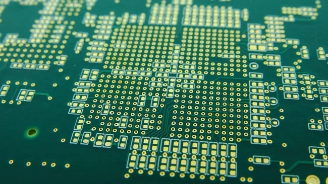
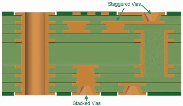
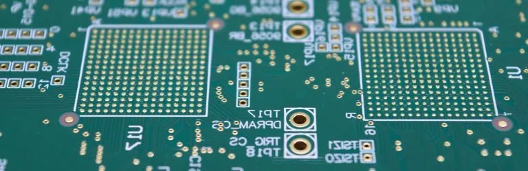
Stacked vias are vertical interconnects placed directly on top of each other to connect multiple layers in a printed circuit board (PCB). Unlike staggered vias, which are offset, stacked vias save space, making them a go-to choice in HDI designs where every square millimeter counts. They enable dense layouts and support high-speed signal transmission by shortening interconnect paths.
However, their compact nature can introduce risks. Poor design or manufacturing can lead to issues like signal degradation, thermal stress, or even structural failure. For instance, a misaligned stacked via might cause a 20% increase in signal loss at high frequencies above 5 GHz. Reliability is critical, especially in applications where failure isn't an option. Let’s explore how to address these challenges with advanced techniques.
Key Challenges in Stacked Via Reliability
Before diving into solutions, it's important to understand the common problems associated with stacked vias:
- Thermal Stress: Repeated heating and cooling cycles can cause micro-cracks in stacked vias, especially if materials with mismatched thermal expansion coefficients are used.
- Signal Integrity Issues: Improper via placement or sizing can lead to parasitic inductance and capacitance, degrading signal quality at high speeds (e.g., above 10 Gbps).
- Manufacturing Defects: Misalignment during drilling or plating can weaken the via structure, reducing reliability over time.
- Structural Weakness: Stacked vias, due to their vertical alignment, are more prone to mechanical stress during assembly or operation.
Addressing these challenges requires a combination of smart design practices and precise manufacturing. Below, we outline advanced techniques to boost stacked via reliability in your HDI PCB projects.
Advanced Design Techniques for Stacked Via Reliability
1. Optimize Via Aspect Ratio
The aspect ratio of a via—its depth divided by its diameter—plays a big role in reliability. For stacked vias in HDI designs, aim for an aspect ratio below 1:1. A lower ratio, such as 0.8:1, ensures better plating uniformity during manufacturing, reducing the risk of voids or weak connections. For example, a microvia with a diameter of 0.1 mm should ideally not exceed a depth of 0.08 mm per layer.
Why does this matter? High aspect ratios can lead to uneven copper deposition, causing weak spots that fail under thermal or mechanical stress. Use simulation tools during the design phase to verify the aspect ratio and adjust layer thickness if needed.
2. Use Via-in-Pad and Blind Via Configurations
Via-in-pad and blind via techniques can enhance reliability by reducing the stress on stacked vias. Placing vias directly under component pads minimizes routing length, which cuts down on signal loss and parasitic effects. Blind vias, which don’t pass through the entire board, also reduce the number of stacked connections, lowering the risk of failure.
For high-speed designs operating at 10 Gbps or more, via-in-pad can reduce signal reflection by up to 15%. Ensure proper pad sizing to avoid solder wicking during assembly, which can compromise the via structure.
3. Implement Proper Stacked Via Alignment
Misalignment in stacked vias is a common cause of reliability issues. Even a slight offset of 0.05 mm between layers can create stress points that lead to cracks over time. Use advanced design software with built-in alignment checks to ensure precision during layout. Additionally, limit the number of stacked vias to 2-3 per connection in critical areas to minimize cumulative misalignment risks.
Work closely with your fabrication partner to confirm their alignment tolerances, as manufacturing precision directly impacts via reliability. Many modern facilities can achieve alignment accuracy within 0.02 mm, which is ideal for HDI designs.
Material Selection for Enhanced Reliability
1. Choose High-Quality Dielectric Materials
The dielectric material between PCB layers affects how stacked vias handle thermal and mechanical stress. Materials with low coefficients of thermal expansion (CTE), such as high-Tg FR-4 or polyimide, are excellent choices for HDI boards. A CTE mismatch between the via copper (around 17 ppm/°C) and the dielectric can cause delamination or cracking during temperature cycles from -40°C to 85°C, common in automotive applications.
Opt for materials with a CTE below 50 ppm/°C and a glass transition temperature (Tg) above 170°C to ensure stability in harsh environments. This reduces the risk of via failure by up to 30% under thermal stress testing.
2. Use Copper-Filled Microvias
Filling microvias with copper instead of leaving them hollow or using conductive paste improves both thermal and electrical performance. Copper-filled vias dissipate heat more effectively, reducing hotspot formation around stacked vias. They also provide a stronger mechanical bond, lowering the chance of cracks during board flexing or vibration.
For high-reliability applications like aerospace, copper-filled vias can increase the mean time to failure (MTTF) by 25% compared to unfilled vias. Coordinate with your manufacturer to ensure proper filling techniques are used, as incomplete fills can introduce new risks.
Manufacturing Processes to Boost Stacked Via Reliability
1. Leverage Laser Drilling for Precision
Traditional mechanical drilling often lacks the precision needed for microvias in HDI designs, leading to rough edges or misalignment in stacked vias. Laser drilling, on the other hand, offers superior accuracy, creating clean, uniform holes as small as 0.075 mm in diameter. This precision reduces stress concentration points, improving long-term reliability.
Laser-drilled vias also have smoother walls, which enhances copper plating adhesion. This can cut defect rates by up to 40% in high-density boards. Ensure your fabrication process includes laser drilling for critical stacked via structures.
2. Focus on Plating Quality
The copper plating process is critical for stacked via reliability. Poor plating can result in voids or thin walls, weakening the via and causing electrical failures. Insist on a plating thickness of at least 20 micrometers for microvias to ensure robust connections. Advanced techniques like reverse pulse plating can improve uniformity, especially in high-aspect-ratio vias.
Regular quality checks, such as X-ray inspection, during manufacturing can detect plating defects early. A well-plated via can withstand over 1,000 thermal cycles without failure, compared to just a few hundred for poorly plated ones.
3. Implement Post-Manufacturing Testing
After fabrication, thorough testing is essential to verify stacked via reliability. Techniques like microsection analysis can reveal internal defects, while thermal cycling tests (e.g., -55°C to 125°C for 500 cycles) assess performance under stress. Electrical testing for continuity and impedance—aiming for values below 50 milliohms per via—ensures signal integrity.
Testing isn’t just a final step; it’s a way to refine your design and manufacturing processes. Data from failed tests can guide adjustments, such as tightening alignment tolerances or switching to a different dielectric material.
Best Practices for Long-Term Reliability
Beyond design and manufacturing, consider these practices to maintain stacked via reliability over the product lifecycle:
- Simulate Before Production: Use simulation tools to model thermal, electrical, and mechanical behavior of stacked vias. Identify potential failure points before committing to fabrication.
- Limit Stack Height: Avoid stacking more than three vias unless absolutely necessary. Higher stacks increase stress and manufacturing complexity.
- Collaborate with Manufacturers: Share detailed design files and discuss reliability goals with your fabrication partner to align on processes and materials.
- Monitor Environmental Factors: Design with end-use conditions in mind. For example, boards for outdoor applications should prioritize low-CTE materials to handle temperature swings.
Conclusion: Building Reliable HDI PCBs with Stacked Vias
Stacked vias are a cornerstone of modern HDI PCB designs, enabling compact, high-performance electronics. However, their reliability hinges on careful design, quality materials, and precise manufacturing. By optimizing via aspect ratios, using advanced drilling techniques, selecting the right materials, and conducting rigorous testing, you can significantly reduce failure risks. Whether you're designing for consumer gadgets or critical industrial systems, these advanced techniques for improving stacked via reliability will help you achieve robust, long-lasting boards.
Integrating these strategies into your workflow ensures that your PCBs meet the demands of high-speed, high-density applications. Focus on precision at every stage—from design to testing—and you'll build products that stand the test of time.