 ALLPCB


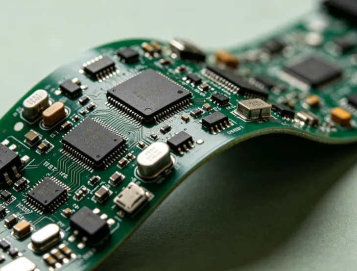
Wearable health devices place unique demands on printed circuit boards because they must operate reliably while subjected to repeated flexing, body heat, moisture exposure, and mechanical shock. Manufacturing defects in these compact assemblies can compromise sensor accuracy, shorten battery life, or cause complete device failure in critical medical monitoring applications.
Engineers therefore focus on identifying and eliminating defects early in the production cycle through structured quality control processes. Effective strategies combine design rules, process controls, and inspection technologies to achieve consistent reliability without excessive cost.
Why Manufacturing Defects Matter in Wearable Health PCBs
Miniaturization required for comfortable wearables increases the density of traces, vias, and components, leaving less margin for process variation. Common defects such as insufficient solder, tombstoning, or board warpage become more likely when substrate thickness drops below 0.8 mm and component pitch falls under 0.5 mm. In health applications, even intermittent opens or high-resistance joints can corrupt biometric data or trigger false alerts. Industry standards therefore emphasize prevention and detection at every stage rather than relying solely on end-of-line testing.
Primary Causes of Defects in Wearable PCB Assembly
Thermal expansion mismatch between components and the substrate is a leading contributor to solder joint cracking during reflow and subsequent thermal cycling. Moisture absorption in laminates can cause delamination or popcorning when boards experience rapid temperature changes in reflow ovens or during device operation near the body. Mechanical stresses from bending and twisting in flexible or rigid-flex constructions further exacerbate micro-cracks that may not appear until after weeks of use. Solder paste deposition inconsistencies on fine-pitch pads also produce bridges or opens that affect signal integrity in sensitive analog front ends.
Process parameters such as reflow profile peak temperature and time above liquidus must be tightly controlled because wearable boards often combine multiple component sizes on the same panel. Variations in stencil aperture design or squeegee pressure can leave insufficient paste on small pads while over-depositing on larger ones, creating both opens and shorts within the same assembly. These issues are compounded when boards undergo multiple reflow passes for double-sided population.
Quality Control Strategies and Inspection Methods
Design for manufacturability reviews performed before fabrication focus on pad geometry, trace routing, and panelization to reduce stress concentrations. Incoming material inspection verifies laminate thickness, copper weight, and surface finish quality against specification. During assembly, solder paste inspection measures volume, area, and height on every pad to catch deposition errors before components are placed.
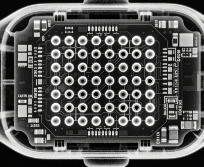
Automated optical inspection after reflow examines component presence, polarity, and gross alignment at high speed, flagging obvious defects for immediate review. For hidden joints such as those under ball grid arrays or chip-scale packages common in compact health modules, X-ray inspection reveals voids, bridges, and insufficient wetting that optical methods cannot detect. Solder joint inspection protocols typically combine these techniques with electrical testing to confirm both visual and functional integrity.
In-circuit and functional testing at the board level verifies continuity, resistance, and basic sensor operation before enclosure integration. Burn-in or accelerated life testing under elevated temperature and humidity conditions helps surface latent defects that might otherwise appear only after field deployment. Statistical process control tracks defect rates by type and location, enabling targeted adjustments to stencil design, reflow profiles, or handling procedures.
Best Practices for Reliable Wearable Health PCB Production
Collaboration between design and manufacturing teams early in the project ensures that component footprints, via placement, and keep-out zones align with achievable process capabilities. Use of IPC-A-610 acceptance criteria provides clear visual and dimensional limits for solder joints, component placement, and board cleanliness. Process validation runs with representative volumes establish baseline capability before full production begins.
Ongoing monitoring of reflow oven profiles and stencil cleaning intervals maintains consistency across batches. When defects are identified, root-cause analysis incorporates cross-sectional analysis or dye-and-pry techniques to understand failure mechanisms and implement corrective actions. These steps reduce the likelihood of field returns and support the high reliability expectations of medical-grade wearable devices.
Conclusion
Reliable wearable health PCBs result from disciplined attention to defect prevention and layered inspection rather than any single technology. Combining design rules, in-process controls, AOI, X-ray, and electrical verification creates multiple opportunities to catch issues before they reach the end user. Adherence to established industry standards guides consistent decision-making across design, assembly, and quality teams. Manufacturers that implement these strategies achieve lower defect rates and higher confidence in long-term device performance.
FAQs
Q1: What are the most common PCB manufacturing defects in wearable health devices?
A1: Common defects include solder opens, bridges, voids, component misalignment, and board warpage caused by thermal and mechanical stresses during assembly and use. These issues arise more frequently in compact, high-density layouts typical of wearable electronics. Early detection through solder paste inspection and automated optical inspection helps maintain yield and reliability.
Q2: How does AOI PCB inspection improve quality in wearable assemblies?
A2: AOI systems scan populated boards after reflow to verify component presence, orientation, and solder fillet quality at production speeds. This method catches visible defects quickly, allowing rework before boards proceed to final test. When combined with X-ray inspection for hidden joints, AOI contributes to comprehensive quality control in health monitoring PCBs.
Q3: Why is X-ray PCB inspection important for health wearables?
A3: X-ray inspection reveals internal solder joint conditions such as voids, bridges, and insufficient wetting beneath components that optical methods cannot see. In dense wearable modules containing ball grid arrays or chip-scale packages, this capability prevents latent failures that could affect sensor accuracy or device uptime. It supports compliance with acceptance criteria defined in relevant industry standards.
Q4: What role does solder joint inspection play in wearable PCB reliability?
A4: Solder joint inspection confirms mechanical and electrical integrity of connections that experience repeated flexing and temperature cycling in body-worn devices. Techniques range from visual and AOI checks to X-ray analysis and cross-sectioning for process validation. Consistent application of these methods reduces the risk of intermittent contacts that could compromise health data collection.
References
IPC-A-610H — Acceptability of Electronic Assemblies. IPC, 2020
J-STD-001H — Requirements for Soldered Electrical and Electronic Assemblies. IPC, 2020
IPC-6012E — Qualification and Performance Specification for Rigid Printed Boards. IPC, 2017


