 ALLPCB


High-density electronic systems in telecommunications, automotive control units, and medical instrumentation increasingly rely on 10-layer printed circuit boards. These multilayer constructions provide the routing density and power distribution planes required for complex signal processing while maintaining controlled impedance. Fabricating a 10-layer PCB introduces process variables that are less critical in simpler boards, including precise layer-to-layer registration, uniform dielectric thickness, and management of cumulative stresses during lamination. Manufacturers address these variables through disciplined process controls aligned with established industry specifications.
What Is 10-Layer PCB Manufacturing and Why It Matters
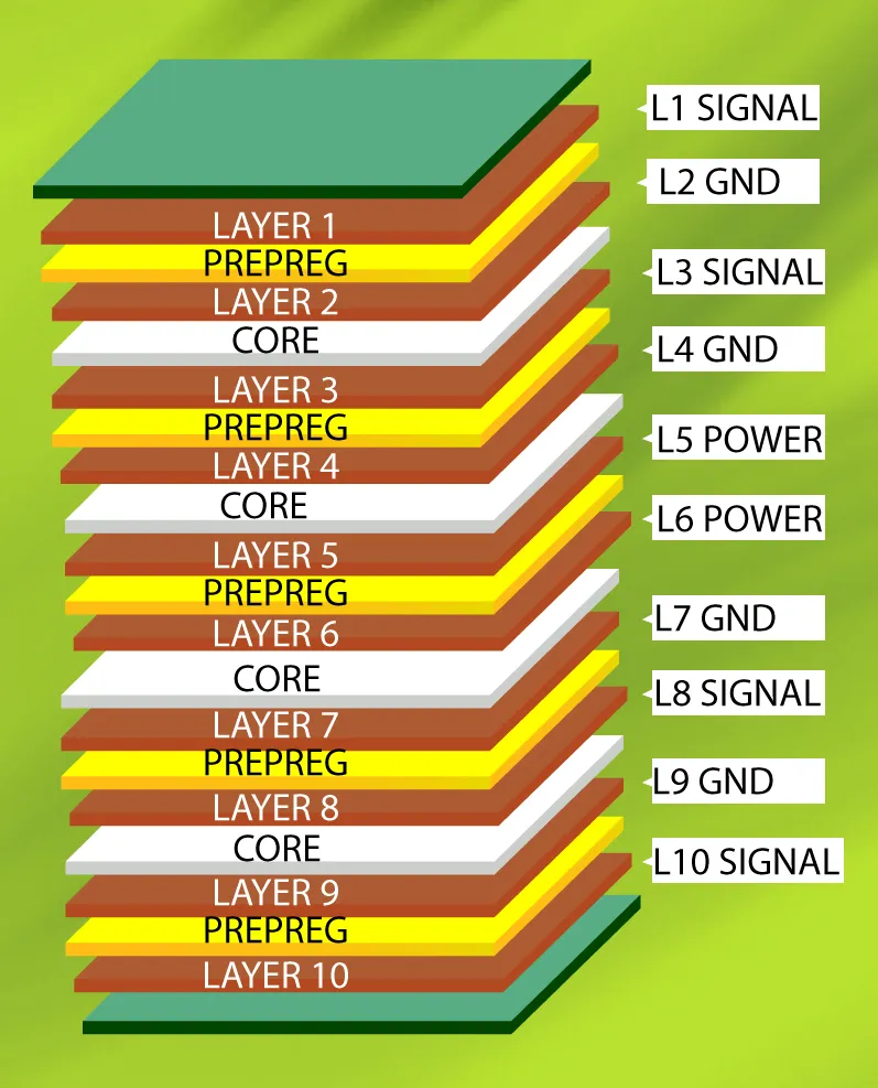
A 10-layer PCB consists of ten conductive copper layers separated by dielectric materials, typically arranged as signal, power, and ground planes. The fabrication process begins with inner-layer imaging and etching, followed by oxide treatment, lay-up, and high-pressure lamination. Subsequent drilling, plating, and outer-layer processing complete the board. This construction supports high-speed digital and mixed-signal designs that cannot be accommodated on fewer layers without compromising performance or increasing board size. Demand continues to grow as electronic assemblies pack more functionality into smaller footprints, making reliable 10-layer PCB fabrication essential for system-level reliability.
Technical Principles and Common Challenges in the 10-Layer PCB Fabrication Process
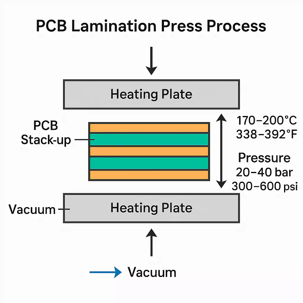
Layer registration becomes increasingly difficult as the number of laminations rises. Each inner layer must align within tight tolerances so that vias connect the intended copper features without shorts or opens. Thermal expansion mismatch between copper and dielectric materials during the multiple press cycles can produce warpage or bow that affects subsequent drilling accuracy.
Resin flow and fill during lamination must be controlled to avoid voids or resin starvation around dense copper areas. Incomplete fill creates potential sites for delamination under thermal or mechanical stress. Copper thickness variation across inner layers also influences impedance and current-carrying capacity, requiring consistent plating and etching parameters throughout the sequence.
Signal integrity considerations further complicate the process. Adjacent signal layers require proper reference planes and controlled dielectric spacing to achieve target impedance values. Any deviation in dielectric thickness or copper roughness introduced during fabrication can shift impedance outside acceptable limits, leading to reflections or crosstalk in high-speed applications.
10-Layer PCB Manufacturing Defects and Their Root Causes
Common defects include misregistration, delamination, resin voids, and excessive warpage. Misregistration often stems from artwork stretch, tooling hole inaccuracies, or differential expansion during lamination. Delamination may result from inadequate surface preparation, moisture absorption in prepreg materials, or excessive thermal stress.
Warpage arises from unbalanced copper distribution or asymmetric stack-up designs that create residual stresses after cooling. These defects directly impact yield and long-term reliability, particularly when boards undergo subsequent assembly processes involving reflow temperatures.
Practical Solutions and Quality Control in 10-Layer PCB Manufacturing
Design rules that balance copper distribution across the stack-up reduce the risk of warpage. Symmetric placement of power and ground planes around the board centerline helps maintain flatness. Material selection focuses on low-CTE laminates and prepregs with consistent resin content to improve registration and minimize voids.
Process controls include automated optical inspection of inner layers before lamination and X-ray verification of registration after pressing. Sequential lamination with intermediate stress-relief steps can further limit cumulative distortion.
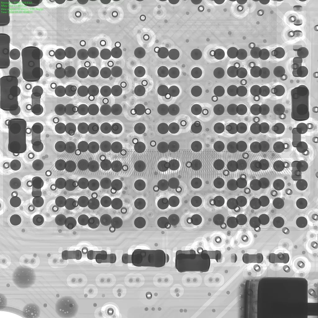
Quality control follows structured inspection protocols. Visual and automated optical inspection at multiple stages, combined with cross-sectional analysis of test coupons, verifies plating thickness, dielectric spacing, and via fill quality. Electrical testing confirms continuity and isolation before boards proceed to final finishing.
Standards such as IPC-6012E provide qualification and performance requirements for rigid printed boards, guiding acceptance criteria for these inspections. Additional guidance appears in IPC-A-600K, which defines acceptability conditions for printed boards. These documents establish consistent benchmarks that manufacturers apply across production lots.
Conclusion
Successful 10-layer PCB manufacturing depends on disciplined control of registration, lamination parameters, and material behavior throughout the fabrication sequence. By addressing the root causes of common defects through design symmetry, process monitoring, and adherence to recognized industry specifications, manufacturers achieve the yields and reliability demanded by complex electronic systems. Ongoing refinement of these practices supports continued advancement in high-density interconnect technology.
FAQs
Q1: What are the primary 10-layer PCB manufacturing defects encountered during fabrication?
A1: Misregistration, delamination, resin voids, and warpage represent the most frequent issues. These defects typically originate from thermal expansion mismatch, incomplete resin flow, or insufficient inner-layer inspection. Systematic process controls and adherence to IPC specifications help reduce their occurrence in production.
Q2: How does the 10-layer PCB fabrication process differ from simpler multilayer constructions?
A2: The 10-layer process requires additional lamination cycles, tighter registration tolerances, and more extensive stress management. Each added layer increases the potential for cumulative distortion and dielectric variation, necessitating enhanced monitoring of alignment and material behavior compared with four- or six-layer boards.
Q3: What quality control measures are most effective for 10-layer PCB manufacturing?
A3: Automated optical inspection of inner layers, X-ray registration verification, and cross-sectional analysis of test coupons provide critical data. Electrical testing and thermal stress evaluations further confirm integrity. These steps, performed at defined process gates, support consistent compliance with acceptance criteria outlined in industry standards.
Q4: Why is material selection important in 10-layer PCB quality control?
A4: Low-CTE laminates and prepregs with uniform resin content minimize warpage and improve layer registration. Consistent dielectric properties also support impedance control. Selecting materials that match the thermal and mechanical demands of the design reduces defect rates during lamination and subsequent assembly.


