 ALLPCB


Electromagnetic interference (EMI) is a persistent challenge in printed circuit board (PCB) design, where unwanted signals can disrupt performance, degrade signal integrity, or cause device failures. For engineers, managing EMI is critical to ensuring reliable electronics, especially in high-speed and high-frequency applications. One of the most effective tools in this battle is the PCB ground plane—a conductive layer that serves as a foundation for stable circuit operation. In this blog, we explore the pivotal role ground planes play in reducing EMI, offering practical insights and design strategies to help engineers optimize their PCB layouts.
Ground planes are more than just a reference point for voltage; they are a shield against noise, a pathway for return currents, and a key factor in maintaining electromagnetic compatibility (EMC). By understanding their function and implementing best practices, you can significantly enhance your PCB's performance. Let's dive into the details of how ground planes work and why they are indispensable in modern electronics.
What Is a PCB Ground Plane?
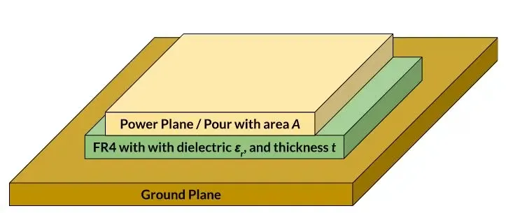
A ground plane is a large, continuous area of copper on a PCB layer, connected to the circuit's ground (0V reference). Unlike individual ground traces, a ground plane spans a significant portion—or even an entire layer—of the board, providing a low-impedance path for return currents. This expansive conductive surface is typically found in multilayer PCBs, though it can also be implemented as a partial layer in single- or double-layer designs.
The primary functions of a ground plane include:
-
Voltage Reference: Offering a stable 0V reference for all components.
-
Return Path: Serving as the return route for signal and power currents.
-
EMI Shielding: Reducing noise and crosstalk by absorbing stray electromagnetic fields.
-
Thermal Management: Dissipating heat from high-power components.
How Ground Planes Mitigate Electromagnetic Interference
EMI occurs when electromagnetic energy from one circuit or device disrupts another, often through radiated or conducted paths. High-speed signals, switching components, and power buses are common EMI sources in PCBs. Ground planes counteract these issues in several ways, making them a cornerstone of EMI reduction.
1. Providing a Low-Impedance Return Path
Every signal in a PCB requires a return path to complete its circuit loop. Without a proper return path, signals can wander, creating noise and radiating EMI. A ground plane offers a low-impedance, direct route for return currents, minimizing loop inductance and reducing the risk of EMI.
For example, in high-speed designs operating above 100 MHz, return currents tend to follow the path of least impedance, typically directly beneath the signal trace. A continuous ground plane ensures this path is uninterrupted, preventing the formation of large current loops that act as antennas. Studies show that a solid ground plane can reduce loop inductance to below 1 nH/cm², compared to 10–20 nH/cm² for routed ground traces.
2. Shielding Against External and Internal EMI
Ground planes act as a Faraday shield, absorbing and dissipating stray electromagnetic fields. By placing a ground plane between two signal layers (a stripline configuration), you can reduce crosstalk by up to 20 dB compared to designs without a ground plane. Similarly, a ground plane on an outer layer (microstrip configuration) protects circuits from external EMI sources, such as nearby devices or power lines.
For instance, in a 4-layer PCB with a stackup of signal-ground-power-signal, the ground plane shields sensitive analog signals from digital noise, ensuring cleaner signal transmission. This is particularly critical in mixed-signal designs, where digital switching can induce noise in analog circuits.
3. Reducing Common-Mode and Differential-Mode Noise
EMI often manifests as common-mode (CM) or differential-mode (DM) currents. CM noise occurs when unwanted currents flow in the same direction on both signal and return paths, while DM noise results from currents flowing in opposite directions. Poor decoupling practices, such as inadequate capacitor placement, can exacerbate these issues.
A ground plane mitigates both types of noise by providing a stable reference and minimizing impedance mismatches. For example, connecting decoupling capacitors directly to the ground plane with low-inductance vias (e.g., multiple vias with 0.1–0.5 nH inductance) can suppress high-frequency noise by up to 30 dB, according to IEEE studies on PCB design.
Best Practices for Designing Effective Ground Planes
To maximize the EMI-reducing benefits of ground planes, engineers must follow specific design guidelines. Below are actionable strategies to ensure your ground plane performs optimally.
1. Maximize Ground Plane Area
The larger the ground plane, the lower its impedance and the more effective it is at reducing EMI. In multilayer PCBs, dedicate an entire layer to the ground plane whenever possible. For single- or double-layer boards, use copper pours to flood unused areas with ground, connected via stitching vias to maintain continuity.
For high-frequency designs (e.g., 1 GHz and above), a continuous ground plane can reduce radiated emissions by 10–15 dB compared to fragmented ground areas. Avoid routing signals over gaps or splits in the ground plane, as these can create slot antennas that radiate EMI.
2. Avoid Splitting Ground Planes Unless Necessary
Splitting a ground plane to separate analog and digital grounds can sometimes reduce noise coupling, but it must be done cautiously. Split planes can act as slot antennas, increasing EMI if signals cross the split. If splitting is required, ensure:
-
Signals do not cross the split.
-
A single-point connection (e.g., a net tie) joins the planes to maintain a unified reference.
-
Vias stitch the planes together to minimize impedance discontinuities.
For most modern designs, a single, continuous ground plane is preferred, with careful component placement to isolate noisy and sensitive circuits.
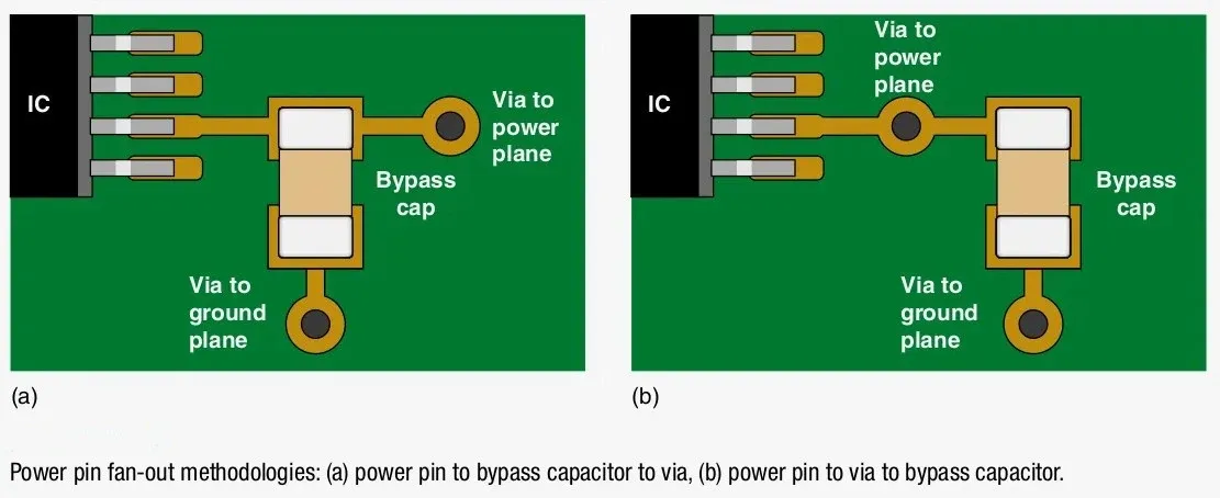
3. Place Decoupling Capacitors Strategically
Decoupling capacitors suppress high-frequency noise by providing a local charge reservoir near power pins. To maximize their effectiveness:
-
Place capacitors as close as possible to the power pins of ICs (within 1–2 mm).
-
Connect the capacitor's ground side directly to the ground plane using multiple low-inductance vias.
-
Use capacitors with low equivalent series inductance (ESL), such as 0.1 µF ceramic capacitors, for frequencies above 100 MHz.
Proper capacitor placement can reduce power bus noise by 20–40 dB, significantly lowering conducted EMI.
4. Optimize Trace Routing
Signal traces are potential EMI sources if not routed carefully. To minimize interference:
-
Route high-speed traces (e.g., clock signals above 50 MHz) adjacent to a continuous ground plane to ensure a clear return path.
-
Avoid sharp 90-degree bends, which increase capacitance and cause reflections. Use 45-degree angles or rounded corners instead.
-
Keep trace lengths short to reduce radiation. For example, a 10 cm trace at 1 GHz can act as an antenna if not properly referenced to a ground plane.
Common Ground Plane Design Mistakes to Avoid
Even with the best intentions, certain design errors can undermine a ground plane's effectiveness. Here are pitfalls to watch out for:
-
Gaps or Slots in the Ground Plane: These create high-impedance paths and radiate EMI. Ensure the plane is continuous, using vias to bridge gaps.
-
Improper Via Placement: A single via may not provide low enough inductance for high-frequency signals. Use multiple vias (e.g., 2–4) for critical connections.
-
Overloading the Ground Plane: High-current components can cause voltage drops if the plane is too thin. Use thicker copper (e.g., 1–2 oz/ft²) for high-power designs.
-
Neglecting Thermal Relief: While thermal relief pads aid manufacturing, they can increase impedance. Minimize their use in high-speed circuits.
By addressing these issues during the design phase, you can prevent costly revisions and ensure EMC compliance.
The Role of Ground Planes in High-Speed and RF Designs
In high-speed digital and radio-frequency (RF) applications, ground planes are even more critical. Signals operating at 1 GHz or higher are highly susceptible to EMI due to their short wavelengths (e.g., 30 cm at 1 GHz). A well-designed ground plane ensures:
-
Signal Integrity: By providing a low-impedance return path, the ground plane maintains clean signal edges, reducing jitter by up to 50 ps in 10 Gbps designs.
-
EMC Compliance: A continuous ground plane can help meet stringent standards like CISPR 32, reducing radiated emissions below 30 dBµV/m at 1 m.
-
Antenna Grounding: In RF circuits, the ground plane serves as part of the antenna system, stabilizing impedance and improving efficiency.
For example, in a 5G module operating at 3.5 GHz, a multilayer PCB with dual ground planes can reduce crosstalk by 25 dB compared to a single-layer design, ensuring reliable data transmission.

How ALLPCB Supports EMI-Optimized PCB Design
At ALLPCB, we understand the challenges engineers face in achieving EMI-compliant designs. Our advanced manufacturing capabilities and quick-turn prototyping services empower you to perfect your ground plane layouts with confidence. Whether you need high-precision multilayer PCBs or rapid iterations to test EMI performance, our global logistics ensure fast delivery without compromising quality. With our expertise in producing boards for high-speed and RF applications, we help you meet EMC standards and bring reliable products to market efficiently.
Conclusion: Building Better PCBs with Ground Planes
Ground planes are a fundamental tool for reducing electromagnetic interference in PCB design. By providing a low-impedance return path, shielding against noise, and stabilizing voltages, they enhance signal integrity and ensure EMC compliance. By following best practices—such as maximizing ground plane area, avoiding splits, and optimizing capacitor placement—you can significantly reduce EMI and improve your PCB's performance.
For engineers working on high-speed, RF, or mixed-signal designs, a well-designed ground plane is non-negotiable. Take the time to plan your ground plane layout carefully, and leverage tools like simulation software to validate your design. With the right approach, you can create robust, reliable PCBs that perform flawlessly in even the most demanding applications.


