 ALLPCB


Printed Circuit Boards (PCBs) are the backbone of modern electronics, and their performance hinges on the quality of their surface finish. Among the various options, Electroless Nickel Immersion Gold (ENIG) stands out for its reliability, excellent solderability, and corrosion resistance. However, for complex PCB designs requiring both soldering and wire bonding or cost optimization, selective ENIG plating offers a tailored solution. This guide dives into the selective ENIG plating process, its benefits, challenges, and best practices, providing engineers with actionable insights to enhance their PCB manufacturing outcomes.
What is Selective ENIG Plating?
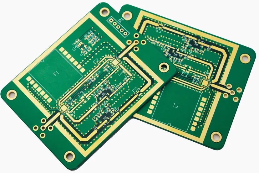
Selective ENIG plating is a specialized PCB surface finish technique where electroless nickel and immersion gold are applied only to specific areas of the board, such as copper pads or traces, while other areas receive alternative finishes like Organic Solderability Preservative (OSP) or Hot Air Solder Leveling (HASL). Unlike standard ENIG, which coats all exposed copper surfaces, selective ENIG targets designated regions to balance performance, cost, and functionality. This approach is particularly valuable in high-density interconnect (HDI) boards or applications requiring diverse assembly methods.
Why Selective ENIG?
Selective ENIG allows manufacturers to optimize costs by limiting the use of expensive gold to critical areas, such as those requiring superior solderability or wire bonding. For instance, a PCB might use ENIG on fine-pitch surface-mount technology (SMT) pads for reliable soldering, while less critical areas receive a cost-effective HASL finish. This flexibility makes selective ENIG ideal for industries like aerospace, medical, and telecommunications, where performance and cost efficiency are paramount.
The Selective ENIG Plating Process
The selective ENIG process involves precise control to deposit nickel and gold only on targeted copper surfaces. Below, we outline the key steps, ensuring clarity for engineers seeking to implement or optimize this process.
1. Surface Preparation and Cleaning
Before plating, the copper surfaces must be thoroughly cleaned to remove contaminants like oxides, oils, or residues from prior manufacturing steps. This typically involves:
-
Degreasing: Using alkaline solutions to eliminate organic residues.
-
Micro-etching: Applying a sulfuric acid or peroxide-based solution to lightly roughen the copper surface, enhancing adhesion for subsequent layers.
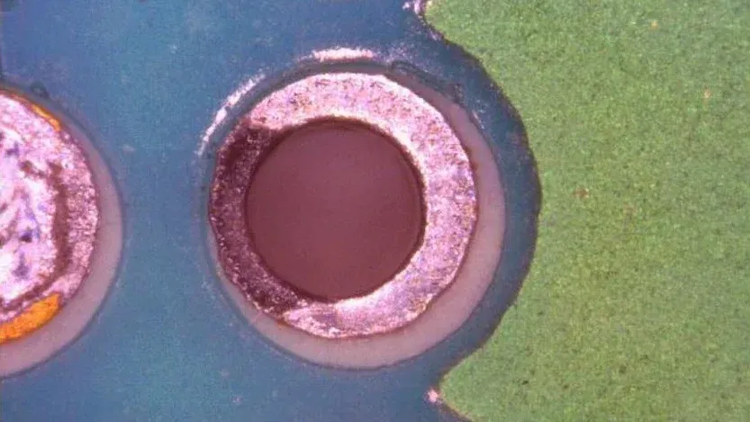
Proper surface preparation is critical, as contaminants can lead to poor adhesion or defects like black pad syndrome, where excessive phosphorus in the nickel layer causes corrosion.
2. Copper Activation
In selective ENIG, the copper areas targeted for plating are activated using a displacement reaction. A chemical solution, often containing palladium chloride, catalyzes the copper surface, preparing it for nickel deposition. Non-targeted areas are masked using a solder mask or temporary resist to prevent unwanted plating.
3. Electroless Nickel Deposition
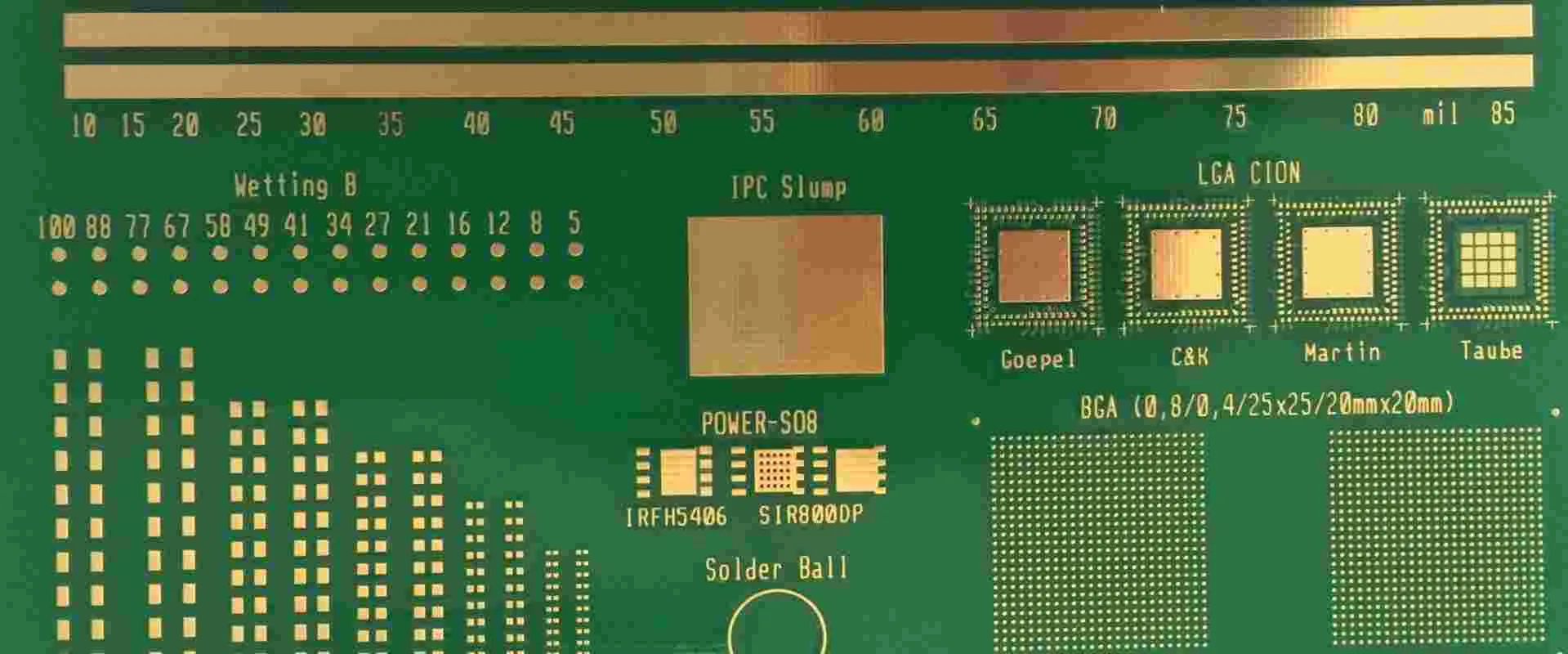
Nickel is deposited via an autocatalytic chemical reaction, forming a uniform layer typically 3-6 µm thick (118.1-236.2 µin), as per IPC-4552 standards. The nickel acts as a barrier layer, preventing copper diffusion and protecting against corrosion. The electroless process ensures even deposition, even on complex geometries, making it suitable for fine-pitch components.
4. Immersion Gold Deposition
A thin gold layer, typically 0.025-0.05 µm (1.2-2 µin), is applied over the nickel via a displacement reaction. The gold enhances solderability and protects the nickel from oxidation. In selective ENIG, precise control of the gold bath chemistry—often containing gold salts like Na3Au(SO3)2—is crucial to avoid deposition on non-targeted areas.
5. Post-Plating Cleaning and Inspection
After plating, the PCB undergoes rinsing to remove residual chemicals. Manufacturers then inspect the board for uniformity, adhesion, and defects like black pad or uneven gold thickness. Advanced techniques, such as X-ray fluorescence (XRF), are used to verify layer thicknesses.
Benefits of Selective ENIG Plating
Selective ENIG offers several advantages, making it a preferred choice for high-reliability applications. Here are the key benefits:
-
Cost Optimization: By limiting gold usage to critical areas, selective ENIG reduces material costs compared to full ENIG plating. For example, gold prices have risen significantly, making selective application a budget-friendly option.
-
Enhanced Solderability: The gold layer ensures excellent solder joint reliability, achieving over 99% first-pass solder joint yields in SMT assembly.
-
Versatility: Selective ENIG supports diverse assembly methods, including SMT, through-hole, and wire bonding, making it ideal for mixed-technology PCBs.
-
Corrosion Resistance: The nickel-gold combination protects copper from oxidation, extending shelf life beyond one year, which is critical for medical and aerospace applications.
-
Surface Planarity: ENIG provides a flat surface, essential for fine-pitch components like Ball Grid Arrays (BGAs) with pitches as low as 0.4 mm.
Challenges and Solutions in Selective ENIG Plating
While selective ENIG is highly effective, it comes with challenges that manufacturers must address to ensure quality.
Challenge 1: Black Pad Syndrome
Black pad occurs when excessive phosphorus in the nickel layer leads to corrosion, weakening solder joints. This is often caused by aggressive gold baths or improper nickel deposition.
Solution: Use modern ENIG chemistries with advanced stabilizers to minimize phosphorus content. Regular monitoring of bath parameters like pH, temperature, and nickel concentration ensures consistent deposition.
Challenge 2: Masking Precision
In selective ENIG, improper masking can lead to gold deposition on unintended areas, increasing costs or causing defects.
Solution: Employ high-resolution solder masks or temporary resists with precise application techniques. Automated optical inspection (AOI) can verify mask alignment before plating.
Challenge 3: Cost Management
While selective ENIG reduces gold usage, the process remains more expensive than HASL or OSP due to the cost of nickel and gold.
Solution: Optimize the design to minimize ENIG-plated areas, reserving them for high-reliability zones. Collaborate with PCB manufacturers to balance cost and performance.
Best Practices for Implementing Selective ENIG
To maximize the benefits of selective ENIG, engineers should follow these best practices:
-
Design for Selective Plating: Clearly define ENIG-plated areas in the PCB design files (e.g., Gerber files) to guide manufacturers. For example, specify ENIG for BGA pads and OSP for through-hole components.
-
Adhere to IPC Standards: Follow IPC-4552 for ENIG thickness and quality specifications to ensure reliability.
-
Optimize Bath Chemistry: Work with manufacturers to maintain stable plating baths, monitoring parameters like pH (typically 4.5-5.5) and temperature (80-90°C) for consistent results.
-
Test for Reliability: Conduct solderability tests (e.g., wetting balance tests) and thermal cycling to verify joint integrity, especially for high-reliability applications like aerospace PCBs.
-
Collaborate with Manufacturers: Engage early with your PCB fabricator to align on design rules, masking techniques, and cost-saving strategies.
Applications of Selective ENIG Plating
Selective ENIG is widely used in industries requiring high reliability and precision:
-
Telecommunications: Ensures stable signal integrity for high-frequency boards with signal speeds exceeding 10 Gbps.
-
Aerospace and Defense: Provides corrosion resistance for PCBs operating in extreme conditions, such as temperatures from -55°C to 125°C.
-
Medical Devices: Supports reliable solder joints for compact, high-density designs in devices like pacemakers.
-
Consumer Electronics: Enables fine-pitch assembly in smartphones and wearables, where space constraints demand pitches below 0.5 mm.
How ALLPCB Supports Selective ENIG Plating
At ALLPCB, we understand the demands of modern PCB manufacturing. Our advanced facilities and expertise in selective ENIG plating enable us to deliver high-quality boards tailored to your needs. With quick-turn prototyping, we can produce ENIG-plated PCBs in as little as 24 hours, ensuring rapid development cycles. Our global logistics network ensures timely delivery, while our stringent quality controls, including XRF and AOI, guarantee compliance with IPC-4552 standards. Whether you're designing for telecommunications, medical, or aerospace applications, ALLPCB's precision manufacturing supports engineers in achieving reliable, cost-effective solutions.
Conclusion
Selective ENIG plating is a powerful technique for balancing performance, cost, and reliability in PCB manufacturing. By targeting specific areas for nickel and gold deposition, engineers can optimize designs for high-density, high-reliability applications while managing costs. Understanding the process, addressing challenges like black pad syndrome, and following best practices are critical to success. With careful design and collaboration with experienced manufacturers, selective ENIG can elevate your PCB projects to meet the demands of today's advanced electronics.


