 ALLPCB


If you're an electrical engineer working on printed circuit boards (PCBs), you might be wondering how to choose the right PCB plating thickness for optimal performance and reliability. The answer lies in balancing factors like signal integrity, durability, and manufacturing constraints. Plating thickness directly affects impedance, signal speed, and the board’s ability to withstand environmental stress. In this blog, we’ll dive deep into PCB plating thickness standards, measurement techniques, its impact on impedance, considerations for high-speed circuits, and calculation methods to help you make informed decisions for your designs.
Introduction to PCB Plating Thickness
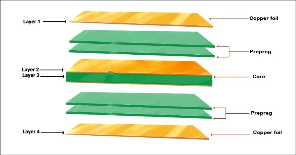
PCB plating thickness refers to the layer of metal, typically copper, applied to the conductive traces, vias, and pads of a printed circuit board. This layer serves multiple purposes: it protects the board from corrosion, ensures good solderability, and maintains electrical conductivity. However, getting the thickness just right is crucial. Too thin, and you risk signal loss or mechanical failure; too thick, and you may face increased costs or impedance mismatches.
For engineers designing high-speed circuits or working on critical applications, understanding how to optimize plating thickness is a game-changer. In this post, we’ll break down everything you need to know about PCB plating thickness, from industry standards to practical tips for calculation and measurement. Let’s get started.
What Are PCB Plating Thickness Standards?
PCB plating thickness standards provide guidelines to ensure consistency, reliability, and compatibility across designs and manufacturing processes. These standards are often set by organizations like the Institute of Printed Circuits (IPC), specifically under standards like IPC-6012 (Qualification and Performance Specification for Rigid Printed Boards).
According to IPC standards, the minimum copper plating thickness for through-hole vias is typically 20 micrometers (μm) or 0.8 mils for Class 2 boards (used in general electronics), and 25 μm (1 mil) for Class 3 boards (used in high-reliability applications like aerospace). Surface finishes, like Electroless Nickel Immersion Gold (ENIG), often have a nickel layer of 3-6 μm and a gold layer of 0.05-0.1 μm to ensure solderability and corrosion resistance.
However, these are just starting points. Depending on your application, you might need to adjust based on factors like current carrying capacity or signal frequency. For instance, high-current designs might require thicker copper (up to 50 μm or more) to handle the load without overheating. Always consult with your PCB manufacturer to confirm their capabilities and adherence to standards, as deviations can impact performance.
How to Measure PCB Plating Thickness Accurately
Measuring PCB plating thickness is a critical step in quality control. If the plating is uneven or outside the specified range, it can lead to failures in signal transmission or mechanical integrity. There are several methods to measure PCB plating thickness, each suited for different scenarios:
- X-Ray Fluorescence (XRF): This non-destructive method uses X-rays to measure the thickness of metal layers. It’s highly accurate (within ±0.1 μm) and commonly used for surface finishes like gold or nickel. XRF is ideal for quick checks during production.
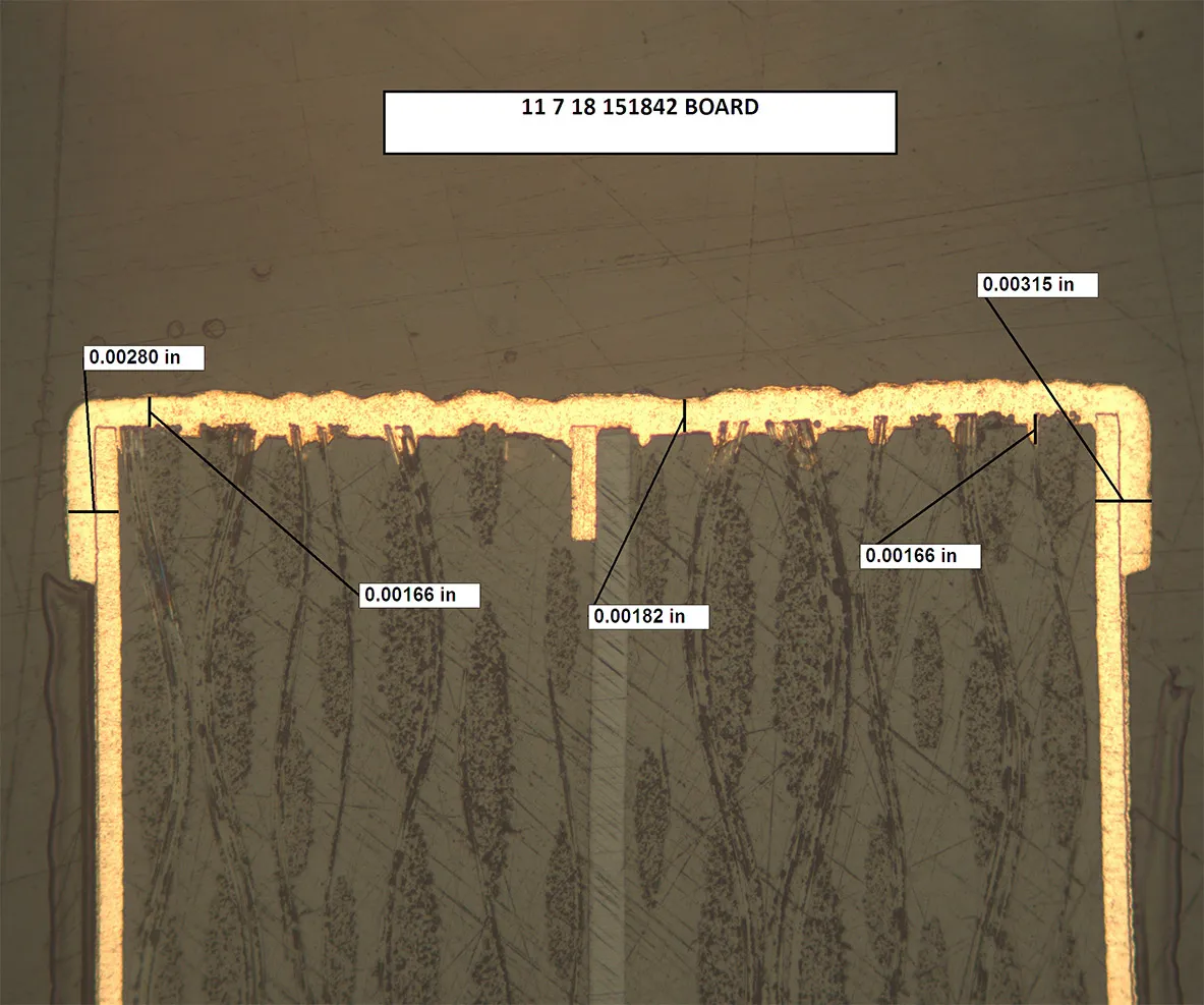
- Cross-Sectional Analysis: This involves cutting a sample of the PCB and examining it under a microscope. While destructive, it provides a detailed view of internal plating in vias and through-holes. It’s often used for failure analysis or validation.
- Eddy Current Testing: This non-destructive technique measures thickness by inducing electrical currents in the conductive layer. It’s useful for copper plating but less effective for very thin layers (below 1 μm).
For engineers, ensuring measurement accuracy means working closely with your manufacturer to define acceptable tolerances. A typical tolerance might be ±10% of the specified thickness, but for high-speed circuits, you might tighten this to ±5% to avoid impedance variations. Regular calibration of measurement tools is also essential to maintain consistency.

Impact of PCB Plating Thickness on Impedance
Impedance control is a critical concern in PCB design, especially for high-speed digital and RF circuits. PCB plating thickness impacts impedance by influencing the conductive path’s geometry and the skin effect at high frequencies.
At high frequencies (above 100 MHz), the skin effect causes current to flow primarily on the surface of conductors. If the plating is too thin, the effective conductor cross-section decreases, increasing resistance and altering the characteristic impedance of the trace. For a typical 50-ohm microstrip line, a copper thickness variation of just 5 μm can shift impedance by 2-3 ohms, potentially causing signal reflections and data errors.
Conversely, overly thick plating can reduce impedance by increasing the conductor’s cross-sectional area, which might require adjustments in trace width or dielectric thickness to maintain the target impedance. This is why precise control over plating thickness is essential for applications like DDR memory or USB 3.0, where impedance tolerances are often ±5% or tighter.
To mitigate these issues, use impedance calculators or simulation tools like Altium Designer or Cadence Allegro during the design phase. These tools can model how plating thickness affects impedance based on your stack-up and material properties, allowing you to fine-tune your design before fabrication.
PCB Plating Thickness for High-Speed Circuits
High-speed circuits, operating at frequencies above 1 GHz, demand special attention to plating thickness due to their sensitivity to signal integrity issues. In these designs, signal propagation speed, loss, and crosstalk are heavily influenced by the conductor and dielectric properties.
For high-speed circuits, copper plating thickness for traces is often kept between 17.5 μm (0.5 oz/ft2) and 35 μm (1 oz/ft2) to balance manufacturability and performance. Thicker copper can reduce resistive losses, but it also increases the risk of over-etching during fabrication, which can distort trace geometry and affect impedance. Vias in high-speed designs may require plating of 25-30 μm to ensure reliable connections without excessive signal delay.
Additionally, surface finishes play a role. ENIG, with its thin gold layer, is preferred for high-speed circuits because it minimizes signal loss compared to thicker finishes like Hot Air Solder Leveling (HASL). However, ensure the nickel underlayer (3-6 μm) is uniform, as variations can introduce parasitic capacitance.
A practical example: In a 5G communication board operating at 28 GHz, engineers might specify a plating thickness of 20 μm for vias to minimize signal delay while using a low-loss dielectric like Rogers RO4350B to complement the design. Close collaboration with your fabricator is key to achieving these precise specifications.

PCB Plating Thickness Calculation Techniques
Calculating the optimal PCB plating thickness involves understanding your design requirements and using tools or formulas to predict performance. Here are some steps and techniques to guide you:
- Determine Current Requirements: For power traces, use the IPC-2221 standard to calculate the required copper thickness based on current and temperature rise. For a 10A current with a 10°C rise, you might need a copper thickness of 35 μm for a 1-inch-wide trace.
- Account for Frequency: At high frequencies, consider the skin depth, which is the depth at which current density drops significantly. Skin depth (in μm) can be calculated as: Skin Depth = 66 / √f, where f is frequency in MHz. For a 1 GHz signal, skin depth is about 2.1 μm, so plating thicker than 5-10 μm offers diminishing returns.
- Use Simulation Tools: Tools like HyperLynx or Ansys HFSS allow you to model plating thickness effects on impedance and signal loss. Input your stack-up details, including dielectric constant (Dk) and loss tangent (Df), to simulate performance.
- Consult Manufacturer Limits: PCB fabricators often have minimum and maximum plating thicknesses they can reliably achieve. For example, many can’t go below 15 μm for via plating due to process limitations.
Let’s walk through a quick example. Suppose you’re designing a USB 3.0 board with a target impedance of 90 ohms for differential pairs. Using a microstrip impedance calculator, you determine that a trace width of 6 mils and copper thickness of 1.4 mils (35 μm) on an FR-4 substrate (Dk=4.2) meets your needs. However, if your manufacturer can only guarantee ±10% thickness tolerance, you might see impedance vary by ±3 ohms, so you adjust the trace width to 5.5 mils to compensate.
These calculations aren’t one-size-fits-all. Always validate with prototypes and testing, especially for critical designs, to ensure the calculated thickness performs as expected in real-world conditions.
Factors to Consider When Optimizing PCB Plating Thickness
Beyond the technical calculations, several practical factors influence how you optimize PCB plating thickness:
- Cost: Thicker plating requires more material and processing time, increasing costs. Balance performance needs with budget constraints.
- Environmental Conditions: Boards exposed to harsh environments (e.g., automotive or industrial) may need thicker plating (30-50 μm) or protective finishes to resist corrosion.
- Manufacturing Tolerances: Not all fabricators can achieve tight tolerances on plating thickness. Discuss capabilities upfront to avoid surprises.
- Signal Integrity Needs: For high-speed or RF designs, prioritize uniform plating to minimize signal reflections and loss.
By weighing these factors, you can strike a balance between performance, reliability, and cost. For instance, a consumer electronics board might use standard 1 oz copper (35 μm) to keep costs down, while a medical device might specify 2 oz copper (70 μm) for added reliability, even at a higher price point.
Common Challenges and How to Overcome Them
Even with careful planning, issues with PCB plating thickness can arise. Here are some common challenges and solutions:
- Uneven Plating: This can occur in vias or complex geometries, leading to weak connections. Solution: Use advanced plating techniques like pulse plating and work with experienced manufacturers.
- Impedance Mismatch: Variations in thickness can disrupt controlled impedance. Solution: Tighten tolerances in your design specs and use simulation tools to predict outcomes.
- Over-Plating Costs: Thicker plating than necessary drives up costs. Solution: Optimize thickness based on current and frequency needs using the calculation methods above.
Addressing these challenges early in the design phase saves time and money. Always perform design reviews and prototype testing to catch issues before full-scale production.
Conclusion: Achieving Optimal PCB Plating Thickness
Optimizing PCB plating thickness is a critical step in ensuring the performance and reliability of your designs. By adhering to PCB plating thickness standards, using accurate measurement techniques, understanding its impact on impedance, tailoring thickness for high-speed circuits, and applying precise calculation methods, you can create boards that meet the demands of modern electronics.
Remember, there’s no universal “perfect” thickness. It depends on your application, budget, and manufacturing constraints. As an electrical engineer, your best tools are collaboration with fabricators, simulation software, and thorough testing. Take the time to analyze your design’s specific needs—whether it’s a high-speed 5G board or a rugged industrial controller—and adjust plating thickness accordingly.


